Phone: +86-755-2357-1819 Mobile: +86-185-7640-5228 Email: sales@ominipcba.com whatsapp: +8618576405228

5G/6G Base Station PCBs: Material Physics and Manufacturing
Addressing insertion loss, thermal density, and signal integrity in 5G/6G infrastructure. A deep dive into low-Dk substrates, hybrid stack-ups, and EMS precision.
PCB TECHNOLOGYPCB MANUFACTURINGPCB ASSEMBLY
OminiPCBA
1/3/20267 min read
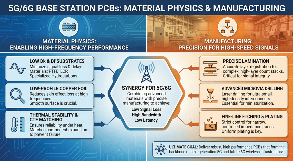
Nowhere is change more clear than in how we build networks for fast signals. Instead of just holding parts together, circuit boards must guide energy with precision. When frequencies climb into ranges used by future systems, even tiny flaws scatter the flow. Materials behave differently under such stress - what worked before fails now. Surface texture matters as much as what lies beneath. Signals travel paths shaped by both chemistry and structure. Not every material keeps pace when demands shift so sharply.
Now electronics makers must rethink old methods. Not just because standards changed, but because tiny shifts matter more than ever. Where once small errors were acceptable, now even micron-level gaps cause problems. It is not about adding precision tools alone - it’s how signals behave on different surfaces. High frequencies push materials beyond their usual limits. What works for one part often fails another under pressure. Seeing this clash helps explain why new base stations need better build choices.
The Physics Behind How Things Spread Using Ordinary Stuff That Doesn’t Hold Up
Frequencies around 28 GHz reveal how materials behave under high-speed signal conditions, shaping choices for 5G AAUs and future 6G transceivers. Signal weakening at such levels comes mainly through energy absorption in insulating layers - dielectric effects take center stage here. Meanwhile, resistance in metal pathways adds further decline, a role played by conductors carrying those fast-moving waves.
Glass fabric soaked in epoxy makes up common FR4, widely used across electronic devices. Its build holds up well under physical stress, yet it carries a dissipation factor between 0.015 and 0.020. Below 6GHz, losses stay within acceptable limits. Once signals climb into millimeter wave ranges, though, those electrically active epoxy parts soak up much more energy. Instead of guiding power smoothly, an FR4 path at 100 GHz behaves like a dead end. Because of this, what works fine for older gear fails completely in next-gen 6G setups.
Because of this shift, companies now push for Ultra-Low Loss substances. Usually built from Polytetrafluoroethylene (PTFE), some rely on custom Hydrocarbon ceramics instead. With Df numbers between 0.001 and 0.003, signals stay strong across long stretches inside big cell towers. But working with them gets tricky - too soft, hard to bore through, plus surfaces reject chemical bonding during plating.
Hybrid Stack Ups Balancing Cost and Performance
A single 5G tower doesn’t just blast radio waves - it juggles complex signal math like a supercharged brain. Instead of carving the whole circuit board from pricey PTFE materials like Rogers or Taconic, engineers avoid that route because twenty layers would cost too much while sagging under its own soft structure.
Here’s where the Hybrid Stack-up comes into play. Built by combining different materials on one multi-layer board, it splits duties smartly. On top, fast radio frequency sections run on costly low-Dk substrates. Below them, digital circuits, power networks, and controls stick to tough high-Tg FR4. Mixing these keeps performance up without breaking cost limits.
The Lamination Challenge
Building hybrid boards takes serious precision in how heat and pressure are managed. Because PTFE expands much more than FR4 when heated, their reactions under stress do not match. During pressing, these materials behave unlike one another - especially as they soften and shift shape. Without exact timing, the stiffer layer might set too soon, trapping voids or blocking proper bonding. Uneven movement while cooling can twist internal connections until they crack. Copper barrels running between layers face extreme strain if expansion pulls them apart sideways. Getting it right means syncing every phase so both materials settle together without fighting each other.
Hitting top production standards means working with smart growth estimates - think Ominipcbas method. When heat shifts materials along the Z-axis, real numbers from test batches guide adjustments in drill patterns and circuit drawings. Because boards pull inward once cooled post-lamination, these tweaks lock alignment tight. Even under shrinkage, radio frequency levels stay lined up with digital traces, never drifting beyond fifty micrometers apart. Precision holds, layer meets layer, without guesswork.
Skin Effect Versus Surface Roughness
Down at DC and lower frequencies, electricity spreads across all of a copper wire's thickness. Moving up toward 5G and beyond, something called Skin Effect pushes current to the edge. When you hit 60 GHz, how deep it goes drops below 0.3 micrometers - almost just a surface skim.
Roughness on copper foil matters more than you might think. Instead of being smooth, standard ED copper carries bumpy peaks that help it stick better to resin. When signals move at mmWave speeds, those tiny bumps start looking like tall ridges to passing electrons. That extra distance across uneven terrain slows things down, shifting timing in subtle but real ways.
HVLP Copper and Chemical Bonding
Smooth copper surfaces on new circuit boards help reduce signal issues. Yet here's the catch - sticking layers together gets harder. When metal lacks texture, bonds weaken during separation tests. Less grip means higher risk of delamination under stress.
Changing how things work in EMS becomes necessary here. To stick smooth copper onto nonreactive PTFE surfaces, specific bonding chemicals plus oxide-based surface prep come into play. Since 5G needs straight-edged traces instead of slanted ones, watching the etch carefully matters - regular acid methods tend to slope inward. Vertical edges help keep signals clean. Because of that, vacuum-driven etching sees more use these days, cutting down on bounce-back effects.
Heat Control with New Power Materials
Nowhere else does heat build so fast as inside a 5G Massive MIMO AAU. As networks shift toward faster speeds, engineers turn to Gallium Nitride for its edge in power handling. Instead of older silicon parts, these new PAs pack more output into tight spaces. Yet that boost brings intense warmth, hard to move away quickly. Because room is limited, the board beneath stops acting like just a wiring layer - suddenly it must pull heat too. So today's circuit boards do double work: guiding signals while soaking up rising temperatures.
Heat doesn’t move fast enough through standard thermal vias under heavy demand. Now, more companies choose copper coins built right into the board. A shaped piece of copper, like a T or an I, gets pressed or glued into a carved-out spot on the circuit layer, placed just below the power amplifier part.
Coin Integration Accuracy
What makes SMT tricky? It’s how flat things sit. A tiny rise in the copper coin means the GaN part wobbles - just like a playground teeter-totter - breaking some solder links. Sink it too far down, though, and the layer between surfaces grows thicker, slowing heat flow. That extra gap resists cooling more than needed.
Not many realize how tiny gaps under power parts cause big issues. What happens is machines check each metal bump shape while building circuits - precision matters here. Instead of normal heating, some factories pull air out during melting so bubbles cannot form. Heat spots pop up if even a small part of the connection lacks contact. When that occurs, gallium nitride weakens faster than expected in real use.
6G Reaches Toward Terahertz Frequencies
When research shifts into 6G, aiming at bands between 100 GHz and 3 THz, copper and resin start falling short. These frequencies expose flaws hidden before - like how the glass weave within circuit boards creates uneven signal paths. One wire in a pair might run above dense glass fibers; its partner moves above softer resin instead. Because signals move slower through resin than glass, delays appear unexpectedly. Timing slips happen without warning when path differences match half-wavelengths. Even tiny gaps in material layout introduce distortion that grows worse as frequency climbs. Such imbalances were once negligible - now they define system limits.
Glass Core Substrates and Metamaterials
A fresh look at materials has engineers testing glass cores for next-gen 6G systems. With near-perfect shape retention, minimal signal fade, and an ultra-flat finish, it fits tight-pitch circuit patterns well. Yet its fragility poses issues - regular drill methods used in board making tend to shatter it. Instead of forcing old tools into new roles, teams are turning to laser-driven deep etching. This method carves pathways through the glass cleanly, sidestepping tiny fractures that weaken connections.
Metamaterials might show up in 6G systems - human-made setups built to behave unlike anything natural, including bending light backwards. Printing tiny repeating patterns, accurate almost to chip-making levels, makes building these possible. What used to separate circuit board production from silicon-scale assembly now overlaps more each year. Cleanrooms run by electronics manufacturers must stay far purer than standard surface-mount areas ever needed.
Passive Intermodulation PIM The Hidden Noise
Signals sent at high power sometimes collide inside FDD setups, generating stray noise that sneaks into receiving channels. That unwanted byproduct? It's called Passive Intermodulation. When it comes to 5G, receivers are tuned so finely they risk being overwhelmed - blinded even - by these faint distortions rising from ordinary hardware.
What triggers PIM? Often, it's quirks in materials - ferromagnetic bits like nickel hiding beneath plating. Uneven copper removal plays a role too. Sometimes, moisture sneaks into the solder mask, making things worse.
Materials and How They’re Used
PIM fights back when cheap parts sneak into the design - so builders pick special laminates and solders made just for this job. Signal paths stay clear of magnetic stuff, thanks to careful SMT planning. Surface coating? That plays a role too: silver or tin dips beat out gold-over-nickel finishes since nickel stirs up trouble. Gold plating might look good but hides a noisy core.
One thing matters most: catching flaws early through PIM test setups right inside manufacturing flow. Even when a circuit board fits together just right and conducts electricity fine, tiny rust specks on contact points might still break performance limits. Hidden issues like uneven metal crystals in solder can slip past basic checks yet ruin signal clarity later down the line.
Manufacturing Precision Through Smt
Now things get tricky when putting together tomorrow’s signal boards - way past just making the base circuit. Tiny parts rule these 5G millimeter wave setups, getting smaller every cycle. Look around. Everyone uses those speck-sized 01005 resistors now, along with chip-first designs needing glue beneath them.
Shielding and Isolation
Keeping signals separate in packed radio-frequency setups means blocking interference right on the circuit board. Tiny metal boxes get fastened by melting solder around fragile parts. When heat spreads during assembly, those same metal covers act like umbrellas, cooling spots nearby too quickly - leaving connections weak where they should bind solid.
Getting the temperature just right means using methods like vapor phase reflow or multi-zone ovens flooded with nitrogen, so heat spreads evenly. Since silver and similar surfaces lose their edge when exposed to air under heat, the lack of oxygen keeps them intact. Conductivity stays strong where it matters most - on the outer layer - because the metal never burns off mid-process. Without that protective gas blanket, signal performance would drop due to degraded finish quality.
Conclusion
Now materials once ignored get fresh attention because of faster wireless networks on the horizon. Base station circuit boards used to just hold parts together but now must behave like tuned radio devices. Smoother metal surfaces matter more than before since signals travel at extreme speeds. New insulation layers help reduce energy waste across connections. Even heat handling methods shift as power concentrates in tighter spaces. Precision in making these pieces changed how engineers see their role.
One thing clear now - design and making stuff blend together more each day. Working together matters most when picking materials, planning layers, setting up how things go together. Take Ominipcbas example - balancing real-world limits with what can be made shows who leads ahead. Not just software shapes how we connect anymore, it's also how copper lines meet plastic sheets just right.
Related Articles
Contacts
Email: sales@ominipcba.com
Mobile: +86-185-7640-5228
Copyright © 2007-2026. Omini Electronics Limited. All rights reserved.
Head Office: +86-755-2357-1819
Services
Your China turnkey partner for electronics manufacturing. We bridge design to delivery by leveraging the Shenzhen electronics ecosystem for precision engineering and streamlined PCBA supply chain logistics.
Ready to Build?
Get a comprehensive quote within 24 hours.
