Phone: +86-755-2357-1819 Mobile: +86-185-7640-5228 Email: sales@ominipcba.com whatsapp: +8618576405228

Precision Testing & Inspection for Critical Electronics
Ensure long-term reliability and zero-defect performance with Omini PCBA’s advanced electronics manufacturing and quality assurance protocols.
Why Rigorous PCB Testing & Inspection is Non-Negotiable
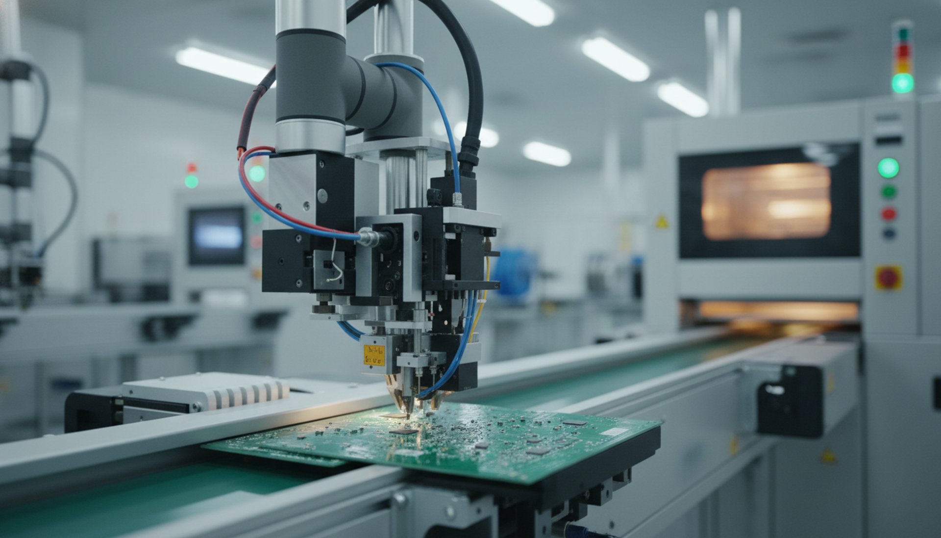
In an era where ultra-fine components and high-density layouts dominate, manufacturing precision is no longer optional. As PCB designs pack more complexity into smaller footprints, even microscopic defects can lead to critical failures. OminiPCBA mitigates these risks by integrating automated optical inspection (AOI) into every production phase. Rather than treating quality as a final step, we embed rigorous verification into our SMT assembly workflow, ensuring long-term product reliability and safeguarding your brand's reputation for excellence.
Full-Spectrum Inspection Technologies
Why Choose Omini PCBA
Today’s PCB designs pack components so tightly—down to 01005 footprints—that manual visual inspection is no longer sufficient. Rather than relying on human sight alone, our SMT assembly process integrates multi-stage automated checks to intercept defects at the source. Utilizing advanced software and 3D AOI (Automated Optical Inspection), every solder joint is measured for volume, height, and alignment. These systems detect flaws hidden by shadows or complex geometries, ensuring every electronic component is oriented perfectly and secured for mission-critical performance.
Hidden interconnects within high-density boards or BGA components require specialized diagnostic tools. Our high-resolution 3D AXI (X-ray) inspection penetrates multilayer stackups non-destructively to identify latent defects like solder voids or bridging. Medical instrumentation and aerospace systems depend on this level of verification where failure is not an option. Beyond visual checks, we validate performance through In-Circuit Testing (ICT) and Flying Probe trials during the prototyping phase. For production runs, custom Functional Testing (FCT) mimics real-world stress—thermal, signal, and mechanical—to ensure total reliability. Strict IPC-A-610 Class 3 standards govern every build, ensuring your hardware thrives in the harshest environments on Earth or beyond.

Our manual soldering specialists are certified to IPC-A-610 standards, ensuring Class 2 and Class 3 reliability for critical devices.

A bed-of-nails approach for high-volume production, testing electrical properties of individual components and trace connectivity.

The ultimate validation. We simulate the actual operating environment to ensure the finished assembly performs exactly as designed.

Ultra-high-resolution cameras compare components and solder joints against CAD data in real-time, detecting missing, misaligned, or incorrect parts.

Perfect for prototypes and low-to-medium volumes. Precise probes verify electrical specs without the need for expensive custom fixtures.

Accelerated aging through thermal stress to detect infant mortality failures in electronic components before field deployment.
Technical Capabilities & Inspection Limits
Precision engineering defines OminiPCBA’s approach to electronics manufacturing, where tight tolerances meet real-world durability. Our facility excels in 01005 (0402 metric) component placement with unmatched consistency, enabling high-density designs to remain robust under stress. Handling ultra-fine pitches down to 0.3mm is standard practice, ensuring your hardware is built for peak performance. We repeat this level of detail reliably across every production batch, from NPI prototypes to high-volume runs.
We accommodate large-format PCBs up to 610mm x 510mm, providing the same precision for both compact devices and heavy-duty industrial controllers. Our quality assurance integrates 3D AXI (X-ray) inspection and flying probe testing with up to 12,000 test points. For power-intensive applications, we conduct high-voltage functional testing—up to 1000V DC and 600V AC—to ensure your circuitry survives demanding real-world environments.
OminiPCBA strictly adheres to global standards, including IPC-A-610 Class 2 and 3 and J-STD-001 for high-reliability assemblies. Our facility is certified to ISO 13485 for medical devices, IATF 16949 for automotive electronics, and ISO 9001 for overall quality management. We ensure full component traceability via unique serialized coding from raw materials to final PCBA. Whether building rugged automotive systems or sensitive medical boards, our data-driven process ensures your technology works perfectly every time.
Built for High-Stakes Sectors
When precision is non-negotiable, OminiPCBA delivers rigorous verification to ensure zero-defect performance. In sectors like aerospace, medical technology, and automotive electronics, reliability is synonymous with safety. Our facility intercepts latent defects using advanced 3D AOI and AXI (X-ray) imaging. These high-resolution tools detect microscopic solder anomalies in high-density PCB assemblies long before field deployment, ensuring your critical systems remain robust.
Beyond visual inspection, we subject every board to In-Circuit Testing (ICT) and custom Functional Circuit Testing (FCT) that replicates real-world operating conditions. This validates signal integrity and thermal management under stress. By adhering to IPC-A-610 Class 3 standards, OminiPCBA transforms complex schematics into ruggedized hardware. We eliminate vulnerabilities through harsh environment simulation and extended burn-in sessions, ensuring your electronics survive everything from industrial floors to orbital missions.
Full component traceability is embedded in our workflow, driven by real-time data rather than assumptions. This level of scrutiny is essential for life-sustaining medical devices and high-performance EV electronics where there are no second chances. At OminiPCBA, technical complexity is met with systematic verification. We don't just claim reliability; we build it into every layer of your PCBA before it leaves our facility.

ISO 13485 compliant assembly for diagnostic, monitoring, and therapeutic devices. Traceability down to the component level.

Ruggedized electronics for EV controls, infotainment, and ADAS systems. Built to withstand vibration and temperature extremes.

Reliable connectivity modules and sensor arrays for smart factories and automation. High-volume, cost-effective production.
High-power PCB assembly for inverters, BMS, and renewable energy infrastructure. Handling heavy copper and thermal management.

Telecom infrastructure relies on signal integrity. High-frequency PCBAs support 5G networks and networking hardware through precision engineering and stability.

Precision-engineered for motion. Specialized robotics PCB assembly optimizes motor control and sensor density, ensuring stability for complex automated hardware.
The Omini PCBA Advantage
Quality is not just a department at Omini; it's our foundational engineering discipline.

Smart Sourcing
Counterfeit detection at intake via specialized component testing.

Full Traceability
Digital records for every component batch and inspection pass.

DFM / DFT Consultation
We design for testability early in the prototype phase.

Rapid Turnaround
In-house fixtures and automated workflows minimize lead times.
Frequently Asked Questions
1.Does Omini PCBA provide functional test fixture design?
Yes. Our engineering team specializes in custom FCT (Functional Circuit Test) fixture development and software integration to mirror your product's actual operating conditions.
2.What is the difference between AOI and X-Ray for my project?
AOI uses visible light to check surface-level assembly (polarities, solder bridges, missing parts). X-Ray (AXI) is required for 'hidden' joints, such as those under BGA chips or in heavy ground plane areas, where visible light cannot penetrate.
3.Can you provide IPC-A-610 Class 3 compliant inspection?
Absolutely. Omini PCBA is fully equipped for Class 3 high-reliability manufacturing, common in aerospace and medical sectors, which includes more stringent soldering and cleanliness standards.
4.What test reports are provided after production?
Every batch comes with a standard Certificate of Compliance (CoC). Detailed AOI/X-Ray heatmaps and functional test logs are available upon request for full traceability.
Contacts
Email: sales@ominipcba.com
Mobile: +86-185-7640-5228
Copyright © 2007-2026. Omini Electronics Limited. All rights reserved.
Head Office: +86-755-2357-1819
Services
Your China turnkey partner for electronics manufacturing. We bridge design to delivery by leveraging the Shenzhen electronics ecosystem for precision engineering and streamlined PCBA supply chain logistics.
Ready to Build?
Get a comprehensive quote within 24 hours.
