Phone: +86-755-2357-1819 Mobile: +86-185-7640-5228 Email: sales@ominipcba.com whatsapp: +8618576405228

Telecommunications PCB Assembly
High-reliability manufacturing for next-generation network infrastructure. From 5G base stations to satellite transceivers, Omini PCBA delivers precision engineering for the connected world.
Advancing Global Connectivity with Precision Manufacturing
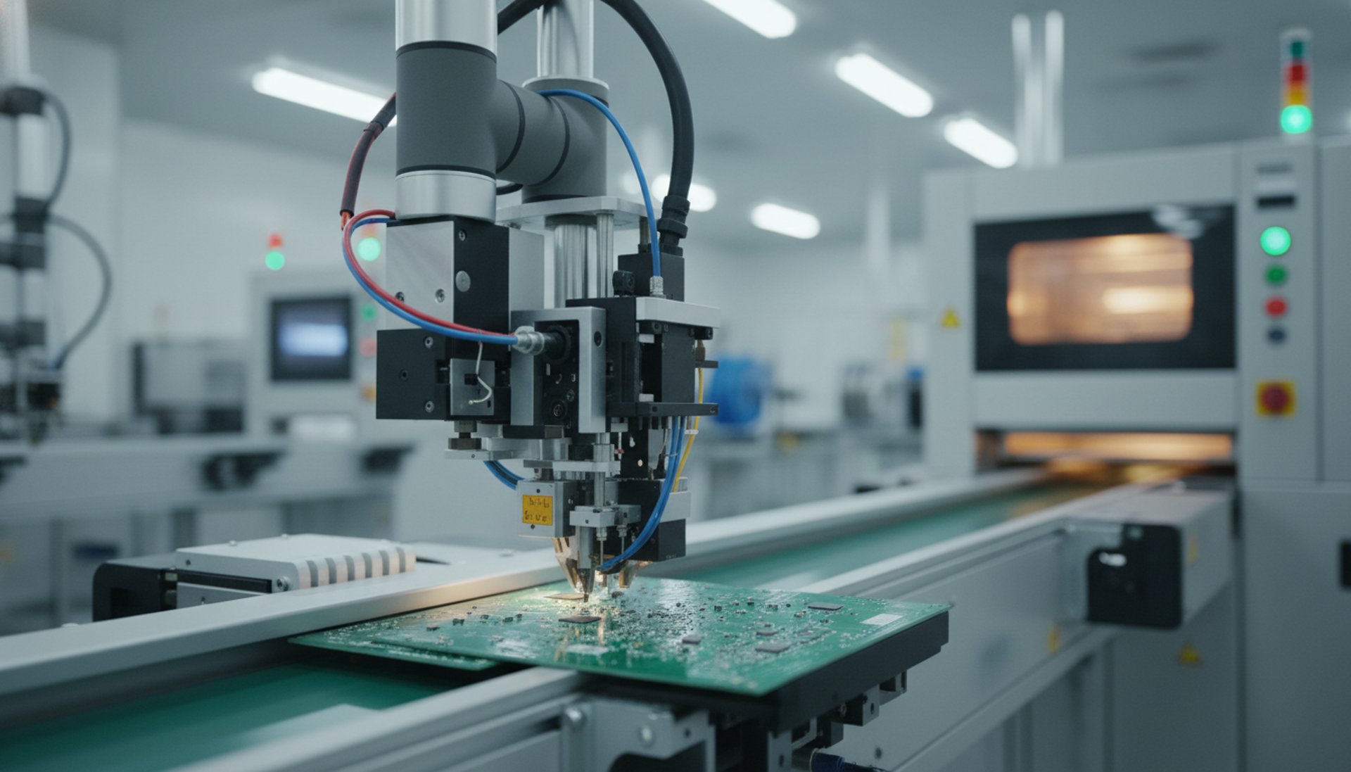
For the next generation of 5G-Advanced and 6G infrastructure, hardware reliability is the foundation of network uptime. OminiPCBA engineers high-frequency PCB assemblies designed to withstand extreme thermal loads and high-speed signal requirements. In the world of wireless telecommunications, where stability is paramount, our boards are built to meet the most rigorous performance benchmarks.
OEM procurement and engineering teams trust OminiPCBA for mission-critical hardware that demands flawless execution. We go beyond basic SMT placement, integrating advanced signal integrity analysis and stable power delivery systems into our EMS manufacturing process. From compact data hubs to high-speed fiber optic units, every board utilizes low-loss laminates and adheres to IPC-A-610 Class 3 standards. The result is rock-solid circuitry that maintains signal purity and operational durability under the most intense network demands.

Expert handling of HDI PCBs for compact industrial devices.
Extreme Environment Durability

Conformal coating and thermal management experts.
PRECISION MANUFACTURING
16+
Years Industry Expertise
Technical Specifications & Capabilities
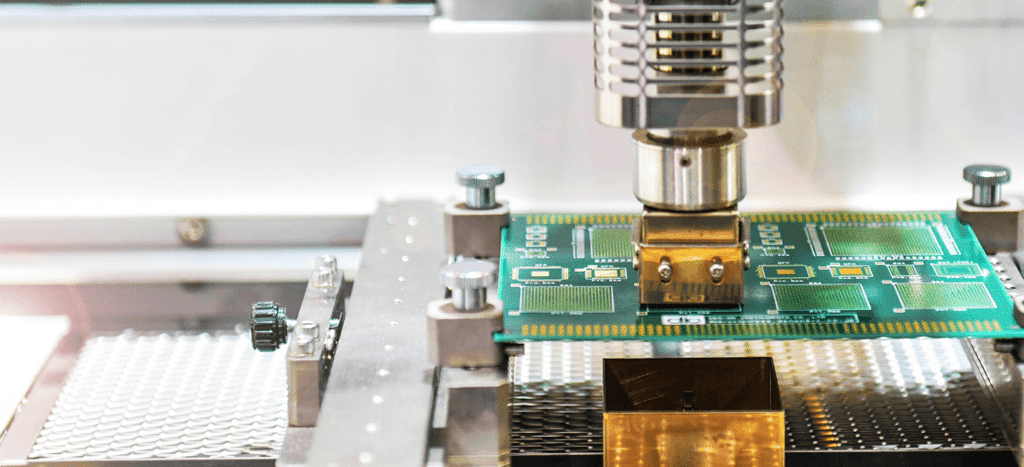
OminiPCBA delivers high-precision PCB assembly engineered for today’s advanced telecommunications and network infrastructure. We specialize in complex multilayer PCBs up to 32 layers, utilizing high-performance substrates like Rogers, Teflon, and Polyimide to ensure superior signal integrity and thermal management. Our HDI manufacturing capabilities support ultra-fine 3-mil traces and the precision placement of 01005 components and 0.35mm pitch BGAs. By pushing technical boundaries, we ensure your high-speed designs achieve peak performance without compromise.
We provide a seamless transition from NPI prototyping to high-volume production, integrating SMT, THT, and mixed-technology assembly. To ensure consistent high-speed data transmission, OminiPCBA maintains a strict impedance tolerance of ±5%, verified across every production batch. Our RoHS-compliant surface finishes—including ENIG, OSP, and Immersion Silver—provide optimal solderability for next-gen wireless and satellite communication hardware. From initial layout to final inspection, we deliver consistent accuracy for the industry's most demanding circuit requirements.
ENGINEERING EXCELLENCE

High Precision 0.3mm Lead Pitch

Thermal Management Optimization

Ruggedized IPC Class 3 Assembly
Why Choose Omini PCBA for Telecom Infrastructure?
Engineered for high-demand 5G infrastructure, OminiPCBA’s telecom PCB assemblies ensure global network uptime with zero latency. We prioritize signal integrity across high-density circuits, managing complex multilayer PCB layouts with absolute precision. Our manufacturing process excels in meeting stringent RF (Radio Frequency) requirements and advanced thermal management, dissipating heat before it impacts performance. For mission-critical telecommunications gear, we deliver the stability and reliability required to perform under intense real-world pressure.
Adhering to IPC-A-610 Class 3 standards is foundational to our production, providing the structural integrity needed for base stations, small cells, and satellite communications. As networks transition to sub-6GHz and mmWave bands, our technical expertise ensures your hardware handles increased frequency demands without signal loss. With comprehensive turnkey EMS support, OminiPCBA transforms sophisticated telecom designs into rugged, field-ready hardware. We build for the future of connectivity—delivered with accuracy, every time.
Specialized handling of Rogers, Taconic, and Nelco materials for RF and high-speed digital applications.
Precision trace width and dielectric height management to ensure signal integrity across complex layers.

01005 component placement and high-density BGA/QFN assembly with automated optical inspection.

Heavy copper, metal core PCBs, and thermal via arrays for high-power base station modules.
Class 3 Reliability

Manufacturing to IPC Class 3 standards for mission-critical aerospace and telecom infrastructure.
Global Supply Chain

Strategic component sourcing to mitigate obsolescence and ensure continuous EMS manufacturing delivery.
CORE COMPETENCIES
Industry Applications
Omini PCBA specializes in the electronics that power our connected world. We understand the specific regulatory and performance hurdles of each sector.
ENGINEERING EXCELLENCE
The Omini PCBA Advantage: Quality Systems & Inspections
OminiPCBA manufactures high-reliability PCB assemblies where durability is the core engineering standard. Recognizing that industrial automation allows zero margin for error, our quality management system is optimized for extreme operational environments. We treat every project as a mission-critical build, utilizing rigorous protocols to ensure your hardware maintains total stability in the most demanding factory settings.
Our IPC-A-610 Class 3 compliant facility specializes in high-precision PLC assembly and smart manufacturing modules. By integrating advanced 3D AOI inspection with full component traceability, OminiPCBA seamlessly transitions your IIoT concepts from NPI prototyping to full-scale production. We don't just assemble boards; we provide the ruggedized hardware foundation required for the future of autonomous industrial operations.

Comprehensive Testing (AOI & X-Ray)
Every board undergoes Automated Optical Inspection. For BGA and complex SMT, 3D X-Ray inspection ensures hidden solder joint integrity.
Material Traceability
Full component and batch traceability systems compliant with industrial and automotive requirements.

DFM Feedback
Our engineers provide free Design for Manufacturing reports to optimize your layout for cost and yield before production starts.
THE OMINI ADVANTAGE
CUSTOMER SUCCESS
Trusted by Global OEM
Frequently Asked Questions
1.What telecommunications certifications does Omini PCBA hold?
Our facilities are ISO 9001:2015 certified, and we follow strict IPC-A-610 Class 3 standards for all telecommunications infrastructure projects. We also offer UL certification support and RoHS compliance as standard.
2.Can Omini PCBA handle high-frequency Rogers or Teflon materials?
Yes, we specialize in high-frequency and RF PCB assembly. We have optimized curing and drilling processes for Rogers, Taconic, Nelco, and other specialized microwave laminates to ensure minimal signal loss.
3.Do you provide turnkey EMS services including component sourcing?
Absolutely. Omini electronics manufacturing offers full turnkey solutions, including global component procurement, PCB fabrication, SMT/THT assembly, and functional testing to deliver a completed product ready for deployment.
4.What is your typical lead time for telecom PCBA?
Prototype runs can be completed in as little as 3-5 days. For mass production of complex telecommunications PCB assembly, lead times typically range from 4-6 weeks depending on component availability and project complexity.
INFORMED DECISIONS
Contacts
Email: sales@ominipcba.com
Mobile: +86-185-7640-5228
Copyright © 2007-2026. Omini Electronics Limited. All rights reserved.
Head Office: +86-755-2357-1819
Services
Your China turnkey partner for electronics manufacturing. We bridge design to delivery by leveraging the Shenzhen electronics ecosystem for precision engineering and streamlined PCBA supply chain logistics.
Ready to Build?
Get a comprehensive quote within 24 hours.
