Phone: +86-755-2357-1819 Mobile: +86-185-7640-5228 Email: sales@ominipcba.com whatsapp: +8618576405228

ABF Substrates: The Strategic Bottleneck of High-Performance Computing
Analyzing the critical role of Ajinomoto Build-up Film (ABF) in HPC hardware, supply chain constraints, and the SMT challenges of assembling advanced IC substrates.
PCB TECHNOLOGYPCB MANUFACTURINGPCB ASSEMBLY
OminiPCBA
1/10/20265 min read
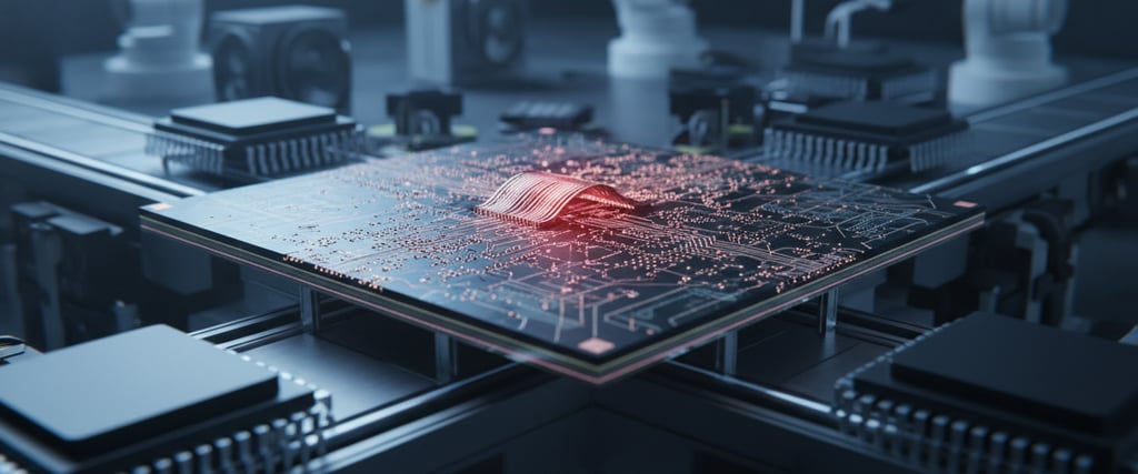
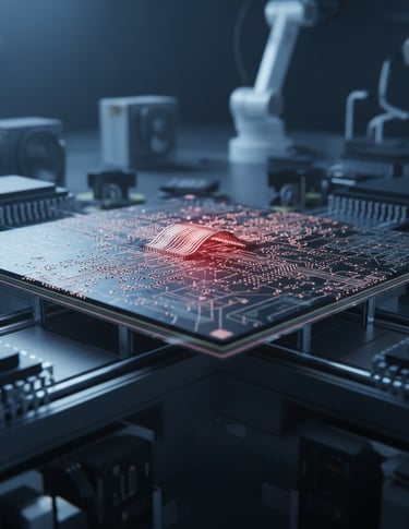
Near the top of today’s electronic tech, one hidden layer pulls more weight than most notice - Ajinomoto Build-up Film, called ABF. When chips shift from single blocks to stacked chiplets, what sits between silicon and circuit boards starts calling the shots on output limits. For machines that power heavy computing tasks, including artificial intelligence tools and next-gen servers, ABF isn’t just another part used up over time. It becomes the base frame holding together how fast logic circuits can run. How easily this film moves through suppliers, plus how precisely it gets layered during assembly, shapes when cutting-edge devices actually ship worldwide.
The Physical Stuff Behind How Computers Work
Picture how tightly ABF controls the market by looking at today’s packaging materials. Start with older types made from Bismaleimide Triazine, often called BT resin. These rely on a mesh of glass fibers for strength. Though tough in structure, that fabric layer creates tiny bumps across the surface. Because of this texture, making very small laser-cut holes becomes difficult.
Unlike others, ABF uses a thin film without any glass fibers. A smooth base forms easily, needed when drawing tiny circuits on today’s processor chips. Without glass in the way, lasers can punch holes smaller than 15 micrometers across. This opens space for more connections packed tighter than older materials allow. Special molecules in the film help ultra-thin copper stick well during processing. That bonding supports techniques shaping lines and gaps narrower than 10 micrometers wide.
Signal quality stays strong on super-fast SerDes connections - those moving data at 112Gbps or more - because the material helps keep things clean. Thanks to its very low dielectric loss, signals lose less strength as they travel from chip to board. Packets move across without turning into static mess by the time they arrive.
The Hidden Trade Off in Production Efficiency
Ajinomoto Fine-Techno dominates much of the film production, yet that’s not where things jam up. Instead, it's the output rate at packaging facilities that really slows everything down. Though people blame limited materials, the real issue hides further downstream. Limited access to ABF films gets mentioned a lot, but actual delays come from how few usable units makers can produce.
Big chips inside computers need huge baseboards, especially ones made for firms such as NVIDIA or AMD - some stretch past 70mm by 70mm, others go beyond 100mm on each side. Built up in stages, these foundations pack anywhere from 18 layers upward, sometimes more than two dozen stacked together.
Start with one step at a time. Building an ABF substrate moves through stages, each depending on the last. A speck of dust shows up now and then. Layers shift out of place once in a while. Tiny gaps form during metal coating more often than expected. Suppose every level works right 99 times out of 100. After twenty rounds, how many make it? Not nearly as many as you’d guess.
A single big server board takes up machine time that could make many tiny phone parts instead. When AI gear gets busy, factories such as Unimicron, Ibiden, and AT&S run nonstop. Machines stay booked solid, pushing wait periods past a year during high seasons.
Supply Chain Stratification
Years ahead, big chipmakers lock down factory space by backing entire assembly lines. Because of that, smaller firms must fight over whatever room remains at suppliers. The ABF material pipeline runs like a ladder - top players grab first dibs, everyone else waits below.
Nowadays, wild swings in supply chains are forcing electronics manufacturers to rethink how they buy parts. The tiny base that holds computer chips can’t just be picked up like regular supplies anymore. Companies building complete circuit boards, including Omnipcba, notice delays often come not from missing processors, but from waiting on special film layers made to order. Because of this shift, teams now fix their plans for those layers long ahead - sometimes even before the chip design finishes - and send orders early to avoid holdups.
SMT Assembly Issues Using Big Substrates
When those valuable ABF substrates arrive on the assembly line, everything gets tense. Each piece carries a steep price, sometimes hundreds of dollars apiece, besides being delicate by design.
Warpage Control
When materials heat up, they grow - but not always by the same amount. That trouble kicks off because the ABF doesn’t stretch like silicon or copper do. Big packages, say over 50 millimeters, start bending noticeably once cooled down. Sometimes they curve upward like a grin, sometimes downward like a frown. Heat them again during assembly, and those shapes flip entirely.
When a board bends too much - more than the tiny space between a BGA ball and the surface - it can break connections or cause wires to touch. That gap is usually just 0.1mm up to 0.2mm tall. Once bent past that point, things stop working right.
Achieving control here means using custom reflow tools or vacuum setups that hold the board steady while pulling out air pockets when the solder melts. Instead of rushing through heat cycles, every bit of the thick substrate warms evenly - yet never so much that the delicate ABF layers burn. Precision isn’t optional; it defines whether the process holds together.
Moisture Sensitivity
Might seem harmless, but ABF pulls in dampness faster than regular FR-4. When heat hits fast during reflow - over 240°C - that soaked-up water doesn’t slip away quietly; it explodes into steam. Pressure builds where it shouldn’t, prying apart layers like a wedge. That split isn’t repairable - called popcorning - shatters reliability without warning
Every part must follow the IPC/JEDEC J-STD-033 rules without exception. Places such as Ominipcba keep components in special dry boxes using powerful moisture absorbers - this stops damp from building up. Only after confirming full dryness do parts move toward assembly machines, held tightly within time limits set by their MSL level.
The Role of Underfill
Down at the tiny scale of chiplets and flip-chips, solder bumps link the die to the ABF base. These fragile connections face strain from movement and heat shifts. A drop of epoxy sneaks into the gap beneath the die. It seals everything, shielding joints from wear over time.
Underfill meeting the ABF layer sets the stage for success. For swift movement through tiny spaces, the ABF surface needs just the right energy level - too low or too high causes trouble. Air pockets form when flow stumbles, then weaken the structure over time. These gaps often spark breakdowns once devices are in use. Watching how fluid gets placed becomes one of the key checks after parts come together.
Future Horizons Beyond Standard ABF
Faster signals mean change. Heading into terabit territory, even common ABF materials aren’t staying the same.
Starting fresh, some updated ABF types - GL102 included - are built to lose less energy. These versions handle signals more cleanly at high speeds. Instead of fading fast, they stay strong where 5G and future 6G operate. Efficiency climbs because internal resistance drops. Materials inside respond quicker without heating up much. One result? Signals travel smoother through circuit paths. Not every grade does this well, but these do.
Twisting under heat, big plastic bases cause trouble - so researchers now eye glass instead. Stiff by nature, it bends less when things get hot. Matched better to silicon’s stretch and shrink, it fits neatly where older materials struggle. Some think this clear stuff could boot out the old core entirely, at least in top-tier setups. Layers on top stay much the same - thin films handling tiny circuits like before. Firmness helps keep everything aligned during assembly. Not a full swap yet, but progress leans that way. Fine details remain handled above, just built smarter underneath.
Conclusion
Out there beneath the spotlight stands the ABF substrate - quiet, essential. Connecting tiny silicon patterns to larger circuit boards is what it does, day after day. Yet shortages pop up, and the stuff cracks if you blink wrong. That shakes the whole system making electronic gear. Progress here depends on timing: chemicals mixed just right, ovens heating chips at exact temperatures. Without getting every small thing correct, building advanced computing machines becomes a lost cause.
Related Articles
Contacts
Email: sales@ominipcba.com
Mobile: +86-185-7640-5228
Copyright © 2007-2026. Omini Electronics Limited. All rights reserved.
Head Office: +86-755-2357-1819
Services
Your China turnkey partner for electronics manufacturing. We bridge design to delivery by leveraging the Shenzhen electronics ecosystem for precision engineering and streamlined PCBA supply chain logistics.
Ready to Build?
Get a comprehensive quote within 24 hours.
