Phone: +86-755-2357-1819 Mobile: +86-185-7640-5228 Email: sales@ominipcba.com whatsapp: +8618576405228

ADAS PCB Manufacturing: Mastering mmWave and LiDAR Precision
Overcoming signal loss and thermal challenges in ADAS sensor manufacturing. A technical guide to hybrid stack-ups, skin effect mitigation, and SMT precision for mmWave and LiDAR.
PCB TECHNOLOGYPCB MANUFACTURINGPCB ASSEMBLY
OminiPCBA
1/2/20263 min read
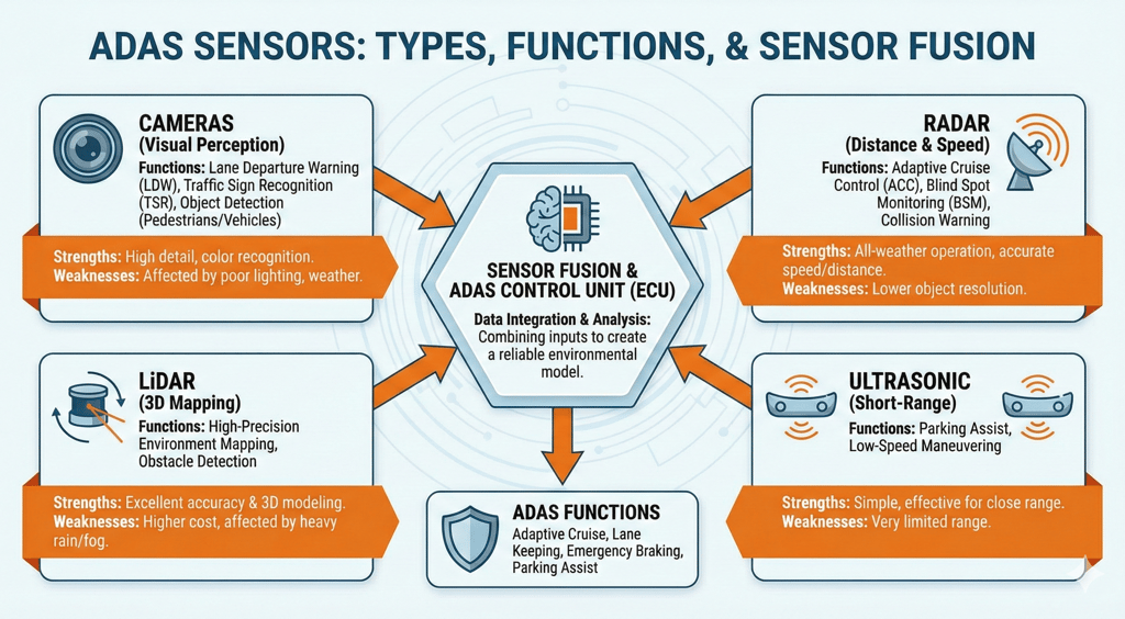
Self-driving vehicles perceive their surroundings through a sophisticated web of light particles and radio frequencies. While software often captures the headlines in ADAS (Advanced Driver Assistance Systems) development, the reliability of these systems is rooted in the physical integrity of the PCBA. High-frequency signals—whether from mmWave radar or LiDAR sensors—require more than just standard manufacturing; they demand a departure from traditional PCB fabrication to ensure signal integrity across every micron.
Why Standard FR4 Fails at 77GHz
At the 77–79GHz frequencies used in modern automotive radar, the physics of signal propagation changes. With wavelengths shrinking to approximately 3.9mm, traditional FR4 substrates become "signal sponges."
Dielectric Consistency: The random glass-fiber weave in FR4 creates inconsistent dielectric constants ($D_k$), leading to unpredictable phase shifts.
Dissipation Factor ($D_f$): FR4’s high dissipation factor causes excessive signal attenuation, rendering long-range detection impossible.
The Solution: High-performance radar PCBs utilize advanced laminates (such as Rogers RO3000 or RO4000 series) that offer stable $D_k$ and ultra-low $D_f$ (under 0.002) to ensure precision in distinguishing pedestrians from stationary objects.
The Hybrid Stack-up Approach
To balance performance with cost-efficiency, Hybrid PCB stack-ups are the industry standard.
Top Layer: PTFE-based or ceramic-filled hydrocarbon materials handle the RF signals.
Inner/Bottom Layers: High-$T_g$ FR4 provides structural rigidity and manages power distribution.
Manufacturing Challenge: Bonding incompatible materials like PTFE and FR4 requires specialized pressing cycles and copper distribution to prevent delamination or warping during thermal cycling.
Overcoming Signal Loss in mmWave Manufacturing
Skin Effect and Copper Foil Profile
In high-frequency bands, electricity crowds the surface of the conductor—a phenomenon known as the Skin Effect. At 77GHz, the skin depth is less than 0.3μm.
Low Profile Copper: Standard "toothed" copper (used for adhesion) increases the signal path length, leading to higher resistive loss. We utilize Very Low Profile (VLP) or HVLP copper to ensure the smoothest possible path for electrons.
Precision Etching
Traditional acid etching creates trapezoidal trace profiles. In mmWave applications, this geometry shifts impedance and causes signal reflection. Our process utilizes vacuum etching and modified chemistry to achieve near-rectangular trace cross-sections, maintaining a strict 50-ohm impedance across the entire signal path.
LiDAR PCBs: Thermal and Inductive Mastery
While radar focuses on signal loss, LiDAR faces challenges in high-current switching and thermal dissipation.
Minimizing Parasitic Inductance: LiDAR diodes (VCSELs) fire nanosecond pulses with peak currents reaching dozens of amps. Even a millimeter of excess trace length acts as an inductor, distorting the pulse shape. We utilize HDI (High-Density Interconnect) technology and stacked microvias to minimize loop inductance.
Thermal Management: To protect sensitive laser diodes, we integrate Copper Coins or Metal Base (IMS) PCBs. These solutions provide a direct thermal path, pulling heat vertically away from the component to prevent wavelength drift or diode failure.
Specialized Surface Finishes for ADAS
The surface finish is an electrical component in high-speed designs.
Avoid ENIG: The nickel layer in Electroless Nickel Immersion Gold is magnetic and increases signal loss at frequencies above 10GHz.
Preferred Finishes: We recommend Immersion Silver (ImAg) or OSP for RF paths to maintain conductivity and flat pad planarity for ultra-fine pitch SMT assembly.
Zero-Defect SMT Assembly for Automotive Safety
ADAS PCBA assembly allows for zero margin of error.
Vacuum Reflow Soldering: To meet automotive standards of <2% solder voiding (compared to the 25% industry standard), we employ vacuum reflow. This eliminates gas pockets under QFN and BGA thermal pads, ensuring optimal grounding and heat transfer.
Cavity PCBs: For ultra-slim sensor modules, components are often mounted within milled cavities. We utilize specialized jet dispensing and custom stencils to ensure precise solder paste deposition in these recessed areas.
Rigorous Testing & Reliability
Every ADAS board undergoes a gauntlet of validation:
Anechoic Chamber Testing: Verification of antenna radiation patterns.
Thermal Shock: Cycling from -40°C to +125°C to ensure via integrity.
Ionic Contamination Testing: Post-wash analysis to prevent electrochemical migration and dendritic growth.
The OminiPCBA Advantage
Manufacturing for the automotive future requires a shift from "commodity board house" to "precision engineering partner." From handling delicate PTFE laminates to achieving micron-level SMT accuracy, OminiPCBA delivers the reliability required for 4D imaging radar and complex sensor arrays. When the goal is autonomous safety, the circuitry underneath must be flawless.
Related Articles
Contacts
Email: sales@ominipcba.com
Mobile: +86-185-7640-5228
Copyright © 2007-2026. Omini Electronics Limited. All rights reserved.
Head Office: +86-755-2357-1819
Services
Your China turnkey partner for electronics manufacturing. We bridge design to delivery by leveraging the Shenzhen electronics ecosystem for precision engineering and streamlined PCBA supply chain logistics.
Ready to Build?
Get a comprehensive quote within 24 hours.
