Phone: +86-755-2357-1819 Mobile: +86-185-7640-5228 Email: sales@ominipcba.com whatsapp: +8618576405228

BGA Design Secrets: A Sourcing Expert’s Guide to Manufacturing in China
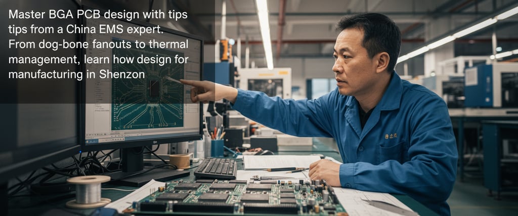
Master BGA PCB design with tips from a China EMS expert. From dog-bone fanouts to thermal management, learn how to design for manufacturing in Shenzhen
PCB TECHNOLOGYPCB MANUFACTURINGPCB ASSEMBLY
OminiPCBA
12/11/20253 min read

For over two decades, we have operated at the intersection of U.S. design logic and Chinese manufacturing precision. Few challenges in the electronics industry are as persistent—or as critical—as the Ball Grid Array (BGA). As devices shrink and pin counts soar, these components have become the backbone of modern hardware, found in everything from smart thermostats to high-performance supercomputers.
In the world of PCB assembly, even a perfect schematic can result in an unbuildable board. Walking the floors of specialized facilities in Shenzhen or Suzhou, it becomes clear that the most common failures aren't due to flawed circuitry, but layouts that ignore the physical realities of the factory floor. Success depends on how well BGA designs align with actual machine tolerances.
Pre-Layout Planning: Designing for Manufacturing (DFM)
Effective BGA integration starts long before the first trace is drawn. Within the Chinese PCB production ecosystem, cost and yield are driven by layer stackup and via architecture.
Prioritize Layer Depth: Generally, fewer high-quality layers are more cost-effective than complex, shallow stacks.
Pin Count vs. Layer Count: A common pitfall is underestimating the layers required for complex routing. For a 0.8mm pitch BGA with 400+ pins, a standard four-layer board is rarely sufficient.
Escape Routing: Plan your "breakout" strategy immediately. While blind and buried vias offer more freedom, they increase costs. If the budget is tight, meticulous pin-exit planning using standard through-hole vias is essential.
Mastering the Fanout: Dog-Bone vs. Via-in-Pad
The strategy used to route traces away from a dense BGA determines the overall reliability of the PCBA.
The "Dog-Bone" Standard
For BGA pitches of 0.8mm or larger, the "Dog-Bone" fanout is the industry standard. This involves a short trace connecting the BGA pad to a diagonally offset via.
Expert Insight: To ensure long-term reliability, maintain a physical separation between the solder pad and the via. This prevents "solder wicking"—where solder is pulled into the via during reflow—ensuring a robust mechanical and electrical connection.
The Via-in-Pad (VIP) Necessity
When the pitch drops to 0.5mm or less, there is no room for traditional fanouts. Designers must utilize Via-in-Pad technology, placing the via directly beneath the solder ball.
The VIPPO Requirement: To avoid assembly defects, these vias must be plugged with epoxy and plated over with copper. This process, known as VIPPO (Via-in-Pad Plated Over), prevents solder from draining into the hole, which would otherwise create "voids" and cause joint failure.
Signal Integrity and Thermal Management
A BGA requires stable voltage and efficient heat dissipation to perform at its peak.
Decoupling Strategy: Place decoupling capacitors as close to the BGA power pins as possible—ideally on the bottom side of the board directly beneath the chip. This minimizes loop inductance, which is critical for high-speed signal stability.
Thermal Vias: High-performance chips generate significant heat. Utilize an array of thermal vias to pull heat away from the BGA and into the internal ground planes.
Material Selection: For high-heat applications, ask your EMS provider about High-Tg (Glass Transition Temperature) FR4. Standard materials can warp during BGA reflow, leading to "Head-in-Pillow" (HiP) defects where the solder ball and paste fail to fuse.
Advanced Inspection and Quality Assurance
Because BGA solder joints are hidden beneath the component, visual inspection is impossible. Robust quality control requires specialized equipment.
When selecting a turnkey PCB assembler in China, verify they provide 3D Automated X-ray Inspection (AXI). While 2D X-rays can catch bridges (shorts), only 3D AXI can identify internal voids or insufficient wetting within the joint. We recommend requiring 100% X-ray coverage for all BGA components in your manufacturing service agreement.
Partner with Omini for Complex PCBA Projects
A design is only as good as the final product that rolls off the assembly line. Omini serves as your expert partner in China, bridging the gap between sophisticated design and high-yield manufacturing.
We specialize in optimizing layouts for seamless Surface Mount Technology (SMT), ensuring that every BGA connection is verified via 3D X-ray. By aligning your vision with our hands-on production expertise, we deliver high-precision electronics while maintaining a competitive cost structure.
Turn your sketches into solid, scalable products with Omini.
Related Articles
Contacts
Email: sales@ominipcba.com
Mobile: +86-185-7640-5228
Copyright © 2007-2026. Omini Electronics Limited. All rights reserved.
Head Office: +86-755-2357-1819
Services
Your China turnkey partner for electronics manufacturing. We bridge design to delivery by leveraging the Shenzhen electronics ecosystem for precision engineering and streamlined PCBA supply chain logistics.
Ready to Build?
Get a comprehensive quote within 24 hours.
