Phone: +86-755-2357-1819 Mobile: +86-185-7640-5228 Email: sales@ominipcba.com whatsapp: +8618576405228

Buried Vias PCB: Elevating High-Density Design & Performance
Optimize complex PCB layouts with buried vias. Understand their advantages in signal integrity, space efficiency, and power delivery for advanced electronics manufacturing.
PCB TECHNOLOGYPCB MANUFACTURINGPCB ASSEMBLY
OminiPCBA
1/15/20264 min read
Packing more power into tinier gadgets keeps pushing engineers to rethink how circuits fit together. When parts crowd closer and signals race at lightning speeds, old-school boards run out of room fast. Instead of sticking to surface paths, some teams now tunnel connections through hidden layers below. Hidden holes bored inside the board open up space where wires once tangled above. These tucked-away links help stack layers smarter, letting complex systems breathe again. With every new generation, squeezing everything tighter means finding clever ways underground. What used to work on flat surfaces must now twist through depth, not just width. Building upward forces changes deep within the material itself. More speed means less margin for error in how electricity travels across tiny gaps. Designs evolve when limits appear - often by going beneath instead of around.
context and technical background
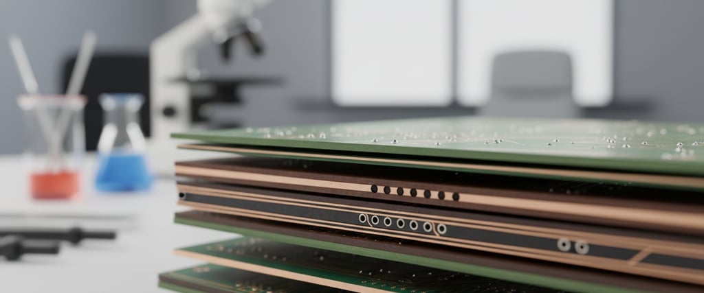
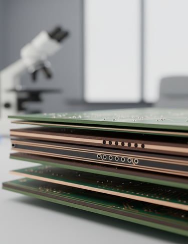
Circuit boards rely on tiny tunnels called vias to link their layered structure together. From the start, most used full-span holes - drilled straight through every level. These older types take up room where other traces could go, crowding tight areas near dense BGA setups. A shift came when makers began capping some links partway down - not reaching the far side. Hidden paths emerged next: built only between inner strata, never seen once sealed inside. With this unique trait, routing management changes completely. Because of it, space on the board gets used much more efficiently. That extra efficiency opens doors to complex circuit layouts. Drilling and plating happen early, focused only on selected inner layers. Only after that comes the next round of laminating.
engineering thoughts and real world methods
Hidden connections inside circuit boards bring real benefits when signals must stay clean, spacing gets tight, or parts pack closely together. Instead of running through every layer like regular holes do, these links join just specific inner levels - cutting down unwanted electrical effects that slow things down at high speeds. Because they avoid extra dangling paths, signals travel clearer, interference drops, and systems handling fast data or radio frequencies work better. They sit out of sight beneath outer surfaces, opening room above for more tracks between chips. Extra space means components fit closer, especially dense ball grid arrays where many pins need escape routes without disturbing nearby lines or power areas. Shrinking devices while keeping power stable becomes easier when hidden pathways handle internal jumps quietly and efficiently.
Starting with core layers already set, machines drill tiny holes where connections will hide inside the board. Once drilled, those holes get coated with metal so signals can pass through. Etching follows, shaping the pathways that link everything together. Next comes heat and pressure - layers of insulating sheets plus fresh copper wrap around the inner sections like a sandwich sealed tight. Each step needs exact alignment; even slight drift throws off later stages. Precision matters most when placing holes, coating them evenly, and stacking every level without shift. Getting clean connections without gaps inside hidden vias takes careful process control - something firms such as Ominipcba handle well, keeping signals stable on crowded boards, especially when holes are narrow and deep. Though harder to build and more expensive, the improvement in circuit behavior and efficient use of space often makes it worthwhile for cutting-edge devices.
Technical Insights Across Industries
Looking at connection methods closely, different via kinds show clear trade-offs when set side by side. Though through-hole versions work well for basic designs with low part counts, they add unwanted signal effects while taking up the most space. Instead of running top to bottom, blind vias cut down leftover wire bits and need less room on outer surfaces, fitting neatly into tighter circuit layouts. With buried ones, signals travel cleaner paths since no stubs get left behind, opening up wiring lanes across every level except where links are made. Tiny spaces on circuit boards matter a lot in powerful computers, medical scanners, flight electronics, and fast networks - here, these connections become essential. Though making them takes more work, like repeated drilling and coating plus pricier materials because of extra layers and special insulating films, they unlock jobs no simpler link could handle. What counts most shows up when nothing else fits the job.
Quality Reliability Long Term Impact
Hidden pathways inside circuit boards must work perfectly if the board is to last. Cracks or gaps in metal coating, thin copper walls, or layers that don’t line up properly might cause signals to flicker or stop completely as time passes. Because of this, every step during making the board follows tight checks - like exact drilling, careful metal buildup, and close examination under magnification. Even tiny details matter; how deep a hole is compared to its width plays a role, just like handling repeated heat changes without breaking down. These unseen links stay strong only when each phase runs smoothly and holds steady through real-world demands. A solidly built hidden connection inside a circuit board helps keep electronic systems stable, plus it cuts down on interference that can cause glitches. Instead of failing early, gadgets last longer because tiny pathways are made right the first time. Fewer returns happen when things work as they should over time. Companies gain trust by delivering products that consistently perform without surprise breakdowns.
Conclusion
Hidden pathways inside circuit boards aren’t just another option - they’re key to making gadgets smaller and faster now. Instead of sticking with old-style holes, engineers use these buried links to solve tight wiring puzzles while keeping signals clean. Through careful placement, they pack more parts into less space without sacrificing stability. Even though building them takes extra effort and precision, the payoff shows up in sleeker, stronger devices. This approach quietly drives progress, letting new tech emerge where size and speed matter most.
FAQ
Q: What are the primary cost drivers associated with using buried vias in a PCB?
A single reason stands out: more layers of materials push prices up. What follows is a unique kind of lamination, not your usual stack-and-press method. Drilling happens multiple times, each round adding to the total. Plating repeats too, step after careful step. Precision becomes critical - alignment must be exact, every time. Air pockets in plating are unacceptable, so margins shrink. Tolerance demands grow strict, limiting room for error.
Q: How do buried vias impact the thermal management of a PCB design?
Even though buried vias are meant for wiring and saving room, they tend to show up in busy circuits that run hotter. They do not move heat any faster on their own, yet opening up top layers means cooling parts fit more easily where needed. With extra breathing room, designers arrange chips and spreaders in smarter ways. This shuffle improves how warmth escapes across the board.
Related Articles
Contacts
Email: sales@ominipcba.com
Mobile: +86-185-7640-5228
Copyright © 2007-2026. Omini Electronics Limited. All rights reserved.
Head Office: +86-755-2357-1819
Services
Your China turnkey partner for electronics manufacturing. We bridge design to delivery by leveraging the Shenzhen electronics ecosystem for precision engineering and streamlined PCBA supply chain logistics.
Ready to Build?
Get a comprehensive quote within 24 hours.
