Phone: +86-755-2357-1819 Mobile: +86-185-7640-5228 Email: sales@ominipcba.com whatsapp: +8618576405228

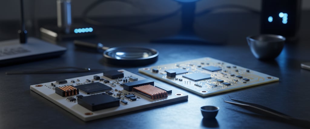
Ceramic PCBs and Alumina PCBs: Exploring the Power
Ceramic circuit boards, alongside those made from alumina, are setting new standards where heat and power push limits. Because they move heat efficiently while blocking electricity reliably, their use grows in tough environments. Over time, these materials prove tougher than many alternatives when stress mounts. In lighting tech, heavy-duty machinery, or complex power setups, they keep things stable. What makes them stand out isn’t just durability - it’s how quietly they enable progress behind the scenes. Their quiet strength is now shaping what future circuits can handle.
PCB TECHNOLOGYPCB MANUFACTURINGPCB ASSEMBLY
OminiPCBA
1/16/202618 min read
1. The Thermodynamic Imperative in Modern Electronics Manufacturing
Right now, what shapes the worldwide electronics scene isn’t innovation for its own sake - it’s packing more into less. Even as circuit patterns dive down to mere billionths of a meter, another shift runs parallel: power chips using stuff like silicon carbide and gallium nitride switch faster, pack tighter currents. Heat becomes the wall everyone hits. Old-school board bases - think fiberglass mixed with epoxy, the kind labeled FR-4 - can’t keep up physically. Their ability to move heat? Stuck near 0.2 to 0.3 watts per meter-kelvin. That means these common layers trap warmth instead of moving it. When systems draw heavy loads, trapped heat pushes internal operating points hotter and hotter. Electrons slow, voltages drift off target, then components die sudden deaths.
Now the big change in electronics making is moving to hard, baked materials instead of soft ones. It isn’t just swapping parts - it’s about needing tougher stuff so new tech like fast wireless gear, strong lights, and powerful circuits can last longer. Out of these tough options, two stand out: one called alumina, another named aluminum nitride. Their ability to move heat ranges between 20 and more than 200 watts per meter-kelvin - way beyond what plastic-like bases could ever handle.
One step at a time, ceramic tech shows how serious makers like Ominipcba take reliability. Though fragile, the base material demands sharp attention - not just during placement but especially when heat reshapes connections. Instead of rushing through steps, working with alumina or aluminum nitride means feeling out each phase: how layers bond, where stress hides, why cooling rates shift outcomes. Every choice echoes across the board, from tiny circuits to final function. Because precision sticks around long after assembly ends, mastering these details separates standard runs from something more exact.
2. Alumina in Material Physics
2.1 Crystal Shapes and Heat Behavior
From the start, alumina - also called aluminum oxide - underpins much of today’s ceramic substrate use because manufacturing methods are well established and it delivers reliable performance without excessive cost. Instead of being rare or exotic, this oxide ceramic appears most often in electronics, commonly at 96% or 99.6% purity. What stands out is how the 96% version dominates applications like thick-film hybrid circuits and those using Direct Bonded Copper setups. Deep inside its makeup, alumina adopts a corundum arrangement, one where oxygen atoms settle into a tightly packed hexagonal pattern. Filling two-thirds of the gaps between them, aluminum ions lock into octahedral spaces. Because of that dense web of ionic and covalent links, the material resists deformation and stays stable when exposed to reactive substances.
Vibrations carry heat through Alumina, much like they do in many non-conducting materials. These tiny vibrations move energy across the material's structure as discrete units called phonons. Even so, the mix of heavy aluminum atoms and light oxygen ones creates disruptions - thanks also to how those ions attract one another - which bounces phonons off course. That bouncing lowers how well heat travels when set beside ceramic types without oxygen. Still, despite that limit, Alumina moves heat far better than common circuit board stuff; think 20 to 30 watts per meter-kelvin versus something barely above 0.25. Because of this trait, warmth gets pulled away from tight clusters of high temperature during everyday operation. Devices like rows of bright LEDs or factory-grade electric changers rely on this feature whenever output rises past what plastic-like supports can handle alone.
2.2 electrical isolation and dielectric behavior
What stands out about Alumina is how well it resists electrical flow. Despite high voltage demands, it maintains stability thanks to resistivity numbers that stay extremely high. Dielectric strength pushes past 15 kV per millimeter, making breakdowns rare. Because of this trait, circuits carrying heavy loads remain safely separated. In power systems, separation between hot components and cooling bases isn’t optional - Alumina delivers it. High potential parts stay cut off from grounded surfaces without fail. Safety and function depend on that barrier staying intact. Electrical isolation like this doesn’t happen by accident. Material choice shapes performance right down to the core. Where heat and electricity collide, one material keeps them apart.
When it comes to radio frequency and microwave uses, how well a material handles electrical signals depends mostly on its dielectric constant and loss tangent. Around 9.5 to 10 - measured at 1 megahertz - is what standard 96 percent alumina offers. Though that number runs higher than most organic materials, which sit between 3 and 4, its real strength lies in staying steady across changing temperatures and frequencies. To cut down signal loss in faster circuits, engineers turn to 99.6 percent pure alumina instead. With less glass-like stuff stuck between the grains, this purer form cuts down energy dissipation. It also creates a more even surface, helping reduce resistance in conductors where current tends to crowd near the edge at high frequencies.
2.3 Mechanical Strength and Building Limits
A hard ceramic, alumina resists bending - its strength sits between 300 and 400 MPa, stiffness near 330 GPa. Because it holds its shape well, surfaces stay flat when placing wires or parts. Yet that same resistance makes it prone to cracking when hit sharply. Sudden force or too much bend often leads to breakage.
One big issue with Alumina in chip packages comes down to how much it expands when heated. Thermal expansion numbers sit around 7–8 ppm/°C - about twice what silicon does, which stays near 3–4 ppm/°C. When devices run hot or cool fast over time, that difference begins pulling on connections. Instead of staying strong, solder points weaken because the materials move out of sync. Cracks can form after repeated stress, breaking electrical contact slowly. Big chips feel this problem more sharply than smaller ones. Because of that, engineers often skip plain Alumina mounts where stability matters most. They might add glue-like underfills, or pick flexible connector designs to absorb strain. Without those fixes, reliability drops too low for critical uses.
3. Aluminum Nitride As A High Performance Thermal Conductor In Material Science
3.1 The Covalent Edge in Phonon Movement
A fresh step forward in heat control comes with Aluminum Nitride. Instead of using oxide-based forms like Alumina, this material links aluminum and nitrogen through tight covalent grips. Its building pattern follows a wurtzite setup - much like what you see in hexagonal zinc sulfide. What makes it work so well? The near-match in weight between aluminum and nitrogen atoms plays a big role. Strong bonds add to the effect. Together, they cut down irregular shaking inside the atomic grid. That lets heat-carrying vibrations move far without getting knocked off track.
Heat moves through this material so well that its ability to conduct warmth sits between 140 and 200 W/mK - some models suggest it could go higher. Compared to Alumina, AlN carries heat seven to ten times better, nearly matching how fast pure aluminum metal transfers heat, yet it still blocks electricity completely. Because of this mix, AlN works like a thermal express lane among non-conductive materials, pulling excess warmth out of heavy-duty parts including laser diodes, radio frequency amps, and IGBT units. Though solid in structure, it behaves almost like a cooling shortcut where insulation is required.
3.2 Matching CTE Ensures Reliable Results
What makes AlN special isn’t just how well it moves heat. Its real strength shows up when materials expand under temperature shifts. Around 4.5 to 5.3 parts per million each degree Celsius - Aluminum Nitride lines up almost perfectly with Silicon at 4.2 and Gallium Arsenide at 5.8. That kind of alignment? It’s what keeps electronic packages stable over time.
Starting with heat, a power module's silicon or silicon carbide chip connects straight to the base through solder. Each time it runs, things warm up. When activity stops, temperatures drop again. Over years, this happens many times. Some bases stretch more than the chip when hot - like those made of alumina or copper do. Because of that mismatch, the solder takes on most of the pull. That repeated load causes stiffening. Tiny breaks appear. Later, layers separate. But aluminum nitride behaves differently. It moves closer in sync with the chip. Less tug means less damage. Stress across the bond shrinks noticeably. For vehicle electric systems and flight electronics, this matters deeply. There, lasting performance despite shifting heat cannot be skipped
3.3 Hydrolysis and Processing Sensitivities
Even though it performs better, Aluminum Nitride can be tricky to work with. Because it reacts if wet, any contact with moisture might cause problems. When water meets AlN powder or open areas, a change happens - Aluminum Hydroxide shows up, along with Ammonia. That shift weakens how well heat moves across the surface. Adhering metal layers later becomes harder because of this altered state
Because of this, places like Omnipcba handling AlN wafers need tight control over their storage environments. Making AlN means baking it hotter than usual while keeping it sealed in nitrogen gas so it does not react with air. That pushes its price well above alumina - one inch costs between five and twenty dollars, while alumina runs three to fifteen. So people pick AlN only when things really can’t fail, even if the material takes more money.
4. Comparative Analysis Engineering the Selection
Not every material handles heat the same way. What holds up under pressure might falter in conductivity. Alumina stands firm where budgets are tight. Yet when precision in signaling matters more than price, Aluminum Nitride often steps forward. Each brings limits as well as strengths into real-world setups.
4.1 The Moment Power Density Shifts
Switching from Alumina to AlN? It usually comes down to how much power gets packed into a space. When levels stay under 50–100 W/, Alumina handles heat well enough - if there's solid cooling nearby. Once numbers rise past 100 W/, things change fast. That’s typical in CPV setups, strong laser diodes, or GaN-based radio frequency parts. Then, Alumina struggles, its resistance to heat flow causing problems. The shift in temperature through the material grows sharp, creating risky hot zones. Because AlN spreads heat better - thanks to higher diffusivity - it smooths out that slope. Instead of stress in one spot, warmth moves freely across the whole base
5. Metallization Technologies Connecting Power
A ceramic base does not conduct electricity. For it to work like a printed circuit board, metal needs to stick to its surface. While regular circuit boards press copper onto resin, ceramics demand stronger connections - something that links two very unlike materials at the atomic level. Instead of glue or pressure, real bonding happens through chemistry or melting. One method bonds thick copper layers right into the ceramic under high heat. Another builds up thin copper using electroplating after initial seed deposition. A third approach uses special metals that react directly with the ceramic when heated in vacuum. Each technique forms stable pathways for current but follows separate physical rules.
5.1 Direct Bonded Copper meets eutectic bonding
A solid method for heavy-duty power setups, Direct Bonded Copper runs on heat-driven chemistry. When things get hot - between 1065°C and 1083°C - a mix of copper and oxygen turns briefly liquid. Foil meets ceramic base before entering a chamber filled with precise gas blends. Temperature holds steady while gases guide the bond. This happens only under tight control of air and warmth
Right around that narrow band of heat - colder than pure copper melts at 1083°C yet warmer than the eutectic kicks in at 1065°C - a delicate film of molten Cu-O appears where surfaces meet. It spreads smoothly, clinging to both the copper sheet and the ceramic face. As things cool down, this fluid joins up with Alumina - or the weathered top of AlN - to build a dense oxide structure ( or ), locking everything together tight, no glue required.14
DBC handles heavy copper well, often between 127 (5 oz) and 800 (23 oz), sometimes even beyond. Because of this dense metal layer, it manages large electrical currents efficiently - perfect for things like IGBT units and power networks. Yet etching those patterns into thick copper relies on liquid-based methods, which blur finer details. As a result, lines and gaps rarely go below 200 , ruling out tight-layout designs. On top of that, exposure to intense heat during manufacturing creates internal pulling forces within the ceramic base. When one side carries much more copper than the other, these tensions may twist the board.
5.2 Direct Plated Copper Precision Through Sputtering
Starting off, when tight connections matter most, copper plating directly on ceramics often stands out. This method borrows tricks from chip making but applies them to sturdy heat-resistant bases. First thing - under strong vacuum conditions - a fine film sticks itself down using vaporized metal like titanium or chromium. Right after that comes a coating of copper, laid thin so later layers bond well. Each step builds quietly, one after another
With a conductive seed layer in place, workers spread on a light-sensitive film. Through exposure to UV patterns, that coating takes shape. Where gaps show up, copper begins forming through an electrical bath process instead of manual placement. After full buildup, what remains is cleaned off carefully by dissolving the template. Underneath, the thin starting sheet vanishes during chemical removal steps.
Starting off, DPC makes it possible to produce very narrow lines and tight gaps - between 20 and 50 - something DBC simply can’t do. Instead of rough textures, you get an even, smooth surface, along with accurate flatness; both matter when attaching wires or chips in LED and radio frequency parts. On top of that, vias with metal lining can be formed through the ceramic, opening paths between layers on both sides - an option rarely seen in regular DBC setups. Yet here's the catch: copper laid down by plating tends to run thin, just 10 to 100 , so handling high currents becomes tricky. Because vacuum-based methods are involved, machines cost more, plus each step takes longer and adds expense
5.3 Active Metal Brazing Sets Reliability Benchmark
Brazed metal activation - called AMB - emerged to fix durability issues seen in DBC when used with ceramics like silicon nitride or aluminum nitride. During manufacturing, a special paste laced with reactive metals - titanium, zirconium, hafnium - gets layered between copper sheeting and the ceramic base
When heated between 800 and 900 degrees Celsius, certain reactive metals interact directly with ceramics, creating a surface layer like titanium nitride. That altered interface allows molten filler metal to spread properly across the joint area. Because of this change, the connection gains strength through chemical bonding rather than just fusion, outperforming traditional DBC methods in durability under stress
Still the top pick for car electronics and motor controllers, AMB sets the benchmark. Though DBC boards often crack or lose copper layers within hundreds of temperature swings (from -55°C up to 250°C), AMB ones keep working through thousands. That toughness matters when using silicon carbide parts in electric cars - those run hotter, shift temps fast. Yet price holds it back; special filler metals and heating methods drive expenses high, limiting use to vital systems only.
6. Working with ceramics in EMS manufacturing
Switching from FR-4 boards to ceramic substrates means Omnicpcba must rethink how things are built. Because ceramics are stiff and tough, they work well - but only if handled just right. Their strength becomes a problem when even small errors cause breakage during assembly.
6.1 Substrate Sourcing and Quality Control
Ceramic substrate production follows a path separate from laminates. Checking each unpopulated piece comes first - workers look closely at tiny cracks, curvature, and flaws on the face. Because ceramics lack flexibility, standard vacuum pressure during assembly won’t straighten warped pieces - one small bend might ruin stencil printing or misalign parts. Before moving forward, many factories scan surfaces with laser-based tools to confirm how level they really are. Flatness matters long before components arrive.
6.2 Depaneling Stress Considerations
Breaking apart tiny circuits from a big board might seem straightforward - yet it carries serious danger. Since ceramic snaps suddenly, without bending first, the move needs extreme care.
Starting off, diamond-coated blades on dicing saws once led the way in cutting ceramic materials. Though clean cuts happen, heavy pressure and shaking come along with them. Heat builds up due to rubbing, so liquid coolant must flow - that brings possible dirt into play. Because of this, extra steps like washing and drying become unavoidable afterward. Edge fractures sometimes begin quietly during slicing, then stretch deeper later, creeping toward working parts inside
Cutting ceramics today often relies on laser ablation instead of physical tools. Using UV or pulsed beams, material gets removed by scoring or full separation. Since there’s no touching involved, the base stays free from mechanical stress. That means less chance for cracks in solder points or the ceramic itself due to shaking. Intricate outlines and curved edges can be formed easily - something straight blades simply cannot achieve. Still, heat from the beam needs precise management. Too much heat in one spot might lead to sudden temperature shifts, creating tiny cracks where the material is cut - the area known as the Heat Affected Zone. Instead of rushing through pulses, some high-end EMS teams fine-tune how long each burst lasts and how often they repeat, shrinking that damaged zone while achieving smooth cuts without internal strain
6.3 Surface Finishes Affect Shelf Life
How smooth the copper layer feels matters a lot when joining parts with solder or attaching fine wires. Sometimes it’s about texture, sometimes chemistry - each detail shifts how well connections form. Without the right top layer, links can weaken or fail entirely. A slight change in finishing alters performance more than expected. What looks like a minor step often decides reliability down the line.
A smooth finish matters when working with dependable ceramic parts - that’s where ENIG comes in. Usually chosen for tough jobs, it layers materials without needing electricity. A coating of nickel, between 3 and 6 microns thick, blocks unwanted material shifts underneath. On top, a flash of gold, just 0.05 to 0.1 microns, keeps air from causing rust. Flatness stands out here, making tiny surface mounts line up cleanly. Wires made of aluminum also stick well thanks to this even base. Parts stay usable for over a year if left on shelves, resisting wear from damp or heat. Corrosion hardly makes a mark under normal conditions. Watch the steps closely though - skip one, and “Black Pad” might show up. That flaw eats away at the nickel zone, weakening connections beneath. Getting every stage right stops trouble before it starts.
With radio frequency uses, Immersion Silver skips the magnetic nickel part that sometimes weakens signals or adds noise. It carries current well and gives a smooth finish good for tight layouts. Yet silver darkens when exposed to air pollution or dampness over time. Parts usually last about half a year before degrading, so they are kept sealed with drying crystals and moisture tags inside special wrap. At Ominipcba, older stock moves out first to keep joints reliable during assembly.
7. The SMT Process Building Assembly on Sturdy Base
Ceramic isn’t like regular circuit boards when it comes to placing tiny parts. Machines need special tweaks just for this material. Settings that work elsewhere often fail here. Adjustments must account for how heat moves through the surface. Tiny shifts matter more than usual. Precision changes are not optional. Each step responds differently compared to common board types. Equipment behaves unlike typical setups.
7.1 Solder Paste Printing and Stencil Design
Right from the start, how well solder paste prints decides much of the build’s outcome. On ceramic substrates, parts crowd together tightly, especially those needing serious power handling. Laser cutting shapes most stencils out of stainless steel, though some get special smoothing - like electro polish or ultra-thin coatings - to help paste let go cleanly.
With ceramic substrates, changes to the aperture layout are usually needed. Since ceramics cannot soak up flux the way certain organic coatings can, while solder refuses to grip the surface, paste amount has to stay exact - too much leads to balls or connections merging. To handle this, step-stencils help apply varied amounts: more for big power pads reducing empty spaces inside joints, less for tightly spaced parts - all on one circuit board.
7.2 Pick and Place Managing Delicate Items
Although it seems harmless, picking and placing parts carries high chances of physical harm. Instead of gentle handling, typical mounting tools made for stiff materials push down too hard on flexible boards. When that happens, especially with brittle ceramics, tiny breaks form without warning inside the material. Even small hits sometimes split delicate pieces such as stacked ceramic capacitors.
Heavy ceramic panels need special vacuum tools to move them safely. Instead of using mechanical clamps, which might crack the material by pressing on edges, vacuum systems offer a gentler option. To protect delicate areas like vias or bond pads, nozzle positions have to skip those zones entirely. When surfaces are smooth - like polished ceramics or DPC copper - they tend to slide easily. Because of this, teams rely on suction cups made for grip, especially when machines shift quickly across rails. Movement precision depends heavily on how well the cup holds during fast motions
A tiny push keeps delicate parts safe during setup. As the machine nears the surface, it eases up - guided by real-time touch signals. Slowing right before landing helps avoid cracks. Most systems apply less than two Newtons of pressure at touchdown. That gentle setting matters most when handling brittle materials like ceramic
7.3 Reflow Profiling Managing Heat Distribution
Ceramics behave oddly in heat, making the reflow oven a tricky spot. Because they warm up fast but store little energy, timing becomes critical inside that space. Adjustments are needed so the process matches how these materials respond - quick to react, slow to hold.
When heated too fast, ceramics risk cracking even if they handle extreme heat well. Temperature jumps cause outer layers to expand faster than inner parts. That imbalance stresses the material. Most circuit boards tolerate quick heating. Big ceramic pieces need care. Providers often limit warming speed to just above one degree per second. Slower increases let heat spread evenly. The material’s natural ability to conduct warmth helps balance everything out. Uneven hot spots fade. Stress drops. Breaks become less likely
Heat moves fast through AlN or Alumina, making the board pull warmth quickly from solder points. Because of this, joints might not melt properly unless enough heat reaches them. Instead of just flowing well, the solder could stay dull and weak when conditions are off. During the phase where flux wakes up, timing plays a big role. How long things stay molten matters just as much. Ovens often run slower on the conveyor so heavy ceramic parts absorb steady warmth. Stronger airflow helps too, balancing how energy spreads across layers. When done right, metal connects smoothly to surfaces meant to hold it
Slowing down matters just as much when things cool off. Fast drops in temperature might tighten up the solder grains on FR-4, yet pull at the ceramic below. Too sharp a cooldown - more than 2 to 3 degrees each second - and tiny cracks may start. Overall, the heat journey takes longer, unfolds softer, stays milder than what you’d see in regular builds
7.4 Avoid Air Pockets With Heat And Pressure
Air pockets stuck in solder joints cause trouble in power electronics. Because they block heat flow, spots get too hot right where the void sits beneath a chip. That heat may damage the device over time. Using regular oven-style heating usually leaves 15 to 20 percent gaps inside big solder areas.
High-end manufacturing fights this issue using Vacuum Reflow Soldering. During the liquid state of solder, air gets pulled out of the oven chamber. Because of the change in pressure, small pockets of gas grow larger, merging together before leaving the hot metal. This method keeps empty spaces under 2% to 5%, which helps heat move better through materials like aluminum nitride or alumina. Providers that handle full assembly often highlight vacuum reflow when working on dense ceramic-based boards.
8. Defects Reliability Failure Modes
8.1 Tombstoning Caused by Uneven Heating of Components
A tiny part might lift at one end when heated, standing like a tombstone. Not flat anymore. Because heat moves unevenly across the board. One side tied to thick copper, another to thin wire. Ceramic soaks up warmth fast - more near big metal zones. So that side stays cooler. Solder melts quicker on the narrow path. It tugs before the other side can join. Pulls the piece into a vertical lean. Balance broken by uneven warmth. Shape shifts mid-melt.
Heat moves fast through big metal areas when soldering. To slow it down, special cutouts around connections help control temperature. These shapes give better results by limiting how much heat spreads too soon. Instead of rushing the process, longer warm-up periods let everything even out first. That way, each joint gets a fair chance to form properly before melting happens
8.2 Solder Fatigue From CTE Differences
Cracks creep in over time when heat shifts stress the joints in ceramic setups. Though AlN lines up well with silicon’s expansion rate, trouble usually starts where the ceramic meets the metal base - copper or aluminum - or where circuit boards connect through solder that just does not stretch the same way.
When temperatures shift back and forth, the parts swell and shrink unevenly. Because of that mismatch, stress builds up over time inside solder connections, making grains grow larger while cracks slowly spread. Even though aluminum nitride helps reduce such effects near the semiconductor die, every layer in the assembly needs to flex just right. With active metal brazed designs, durability tends to improve since the bonding material gives a little under pressure, unlike direct bonded copper setups where stiffness passes force straight into brittle ceramics - often splitting them like glass struck by a hammer.
9. Power and Precision Across Industries
9.1 Car and electric vehicle power systems
Heavy demand for electric vehicles pushes growth in high-performance ceramic materials. Power conversion units take energy from batteries, turning it into usable current for motors - often managing huge loads. Newer designs now use silicon carbide transistors because they manage heat better. These devices also switch faster, improving overall system response.
Starting with mounting, AMB Aluminum Nitride holds the bare SiC dies securely. After placement, sintering or soldering links the setup to a cooling unit that uses liquid. Because AlN resists expansion so well, stress on the die stays low during temperature swings. Over time - think fifteen years or 150,000 miles - that stability keeps cracks away. Without it, the chip might fail long before the car does
9.2 High-Power LED Lighting
Far beyond just brightening sports arenas, today’s LEDs face intense demands - pushed hard in tasks like curing printed materials with ultraviolet light. Power gets packed tighter into these tiny sources, forcing them to operate at levels once thought too harsh.
When bright LED setups run on medium power, alumina usually works fine. Yet when it comes to UV types - less efficient, hotter - a stronger solution kicks in. Tightly clustered COB layouts push heat further, leaving no choice but aluminum nitride. High temps at the core don’t only risk breakdown; they shift color too. Light quality sags unless that internal heat stays under control
9.3 RF and Telecommunications
Frequencies in the millimeter-wave range matter most when 5G links meet radar setups. Signal weakening becomes a key hurdle there.
Heat builds up fast inside GaN transistors when handling radio frequency signals in cell tower equipment. Thin-film circuits often rely on 99.6% pure alumina because it loses little energy as heat. Yet that material struggles to move heat away efficiently. Instead, aluminum nitride steps in where cooling matters just as much as electrical performance. Its ability to transfer heat quickly protects the active components. At the same time, minimal signal loss keeps transmissions clean. So even under heavy load, the system stays stable. Not every insulator can manage both tasks at once. This balance makes AlN stand out in demanding setups
10. What Comes Next
Ceramic circuit boards are changing fast. Though Alumina still wins on price while Aluminum Nitride leads in speed, Silicon Nitride is stepping into the spotlight. Its ability to move heat - around 90 W/mK - fits neatly between the two older materials, yet it handles stress far better than AlN, almost twice as tough. This stuff hardly cracks under pressure. In car power systems, where parts must survive harsh conditions without failing, engineers now lean toward Silicon Nitride when both strength and cooling matter most.
Cooling tech keeps moving forward. Ceramic bases now come with tiny fluid paths built right in, placing the cooling liquid inside the material itself - just a few micrometers away from where heat builds up.
Conclusion
Ceramic circuit boards mark a clear move forward for powerful electronic devices. While alumina stands strong, aluminum nitride brings heat-handling strength that pushes past what standard organic materials can do. Still, just having such a board isn’t enough - success hides in how it gets put together. Working with these materials means teaming up with someone who understands the tricky dance of putting parts on them without flaws.
Ceramics demand care at every stage, so how materials like DBC and AMB bond matters a lot. Because heat shifts subtly during reflow, timing has to match ceramic behavior exactly. At Ominipcba, deep understanding shapes results that go beyond working - they last. When performance cannot fail, such as in aircraft systems or fast-charging cars, using advanced ceramics isn’t new thinking - it’s simply what comes next.
Related Articles
Contacts
Email: sales@ominipcba.com
Mobile: +86-185-7640-5228
Copyright © 2007-2026. Omini Electronics Limited. All rights reserved.
Head Office: +86-755-2357-1819
Services
Your China turnkey partner for electronics manufacturing. We bridge design to delivery by leveraging the Shenzhen electronics ecosystem for precision engineering and streamlined PCBA supply chain logistics.
Ready to Build?
Get a comprehensive quote within 24 hours.
