Phone: +86-755-2357-1819 Mobile: +86-185-7640-5228 Email: sales@ominipcba.com whatsapp: +8618576405228

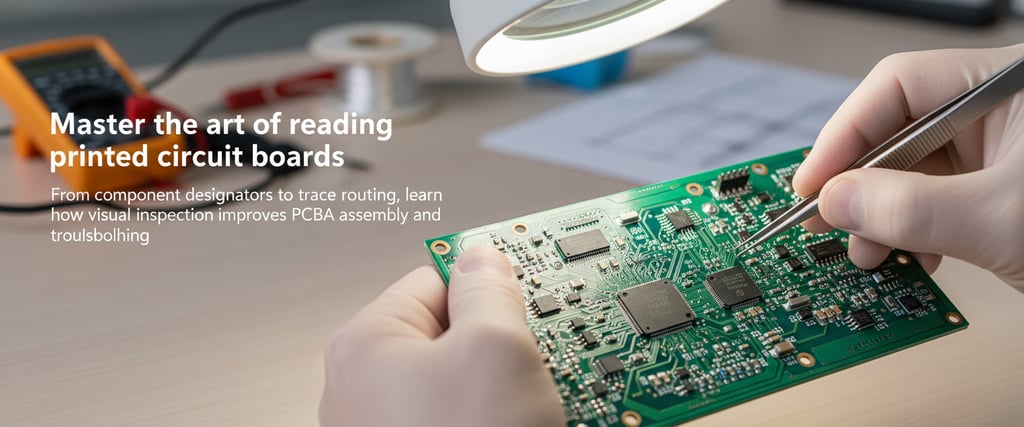
Decoding the Board: A Senior Engineer’s Guide to Reading a PCB
Master the art of reading printed circuit boards. From component designators to trace routing, learn how visual inspection improves PCBA assembly and troubleshooting.
PCB MATERIALS
Amanda
2/5/20253 min read
To the untrained eye, a Printed Circuit Board (PCB) looks like a chaotic city map of green streets and silver structures. But to hardware engineers and procurement professionals, it is a logical, structured document written in copper and fiberglass.
While most of our time is spent analyzing schematics and CAD layout files, the ability to "read" a physical bare board or a fully populated PCBA is a specialized skill. Whether you are debugging a prototype, reverse-engineering a legacy device, or performing a quality check on a production batch, understanding the physical translation of your design is critical for hardware reliability.
Here is how to look past the solder mask and understand the engineering reality of your board.
The Rosetta Stone: Silkscreen and Reference Designators
The first layer of intelligence on any PCB is the silkscreen. Usually printed in white, this layer serves as the primary guide for PCBA assembly teams and rework technicians.
Every component is identified by a Reference Designator (RefDes), following industry standards:
R: Resistors
C: Capacitors
L: Inductors
U or IC: Integrated Circuits
Q: Transistors
D: Diodes
In modern high-density designs, such as those utilizing 0201 components, space constraints often make silkscreen labels impossible. In these cases, we rely on digital assembly drawings or ODB++ files. If a silkscreen is illegible or missing, the PCB manufacturing process becomes significantly more difficult for manual inspection and repair.
Differentiating Board Topologies: SMT vs. Through-Hole
When analyzing a board's physical architecture, you are identifying how components interface with the substrate.
Through-Hole Technology (THT)
These components feature leads that pass through drilled, plated holes. THT is typically reserved for heavy connectors, large electrolytic capacitors, or power components requiring high mechanical bond strength. From a procurement and EMS perspective, THT often increases costs as it may require manual or wave soldering.
Surface Mount Technology (SMT)
The gold standard for modern electronics, SMT components are soldered directly onto surface pads. This allows for high-density population on both the top and bottom layers of the PCB.
Why it matters for troubleshooting: A through-hole pin typically carries a signal through every layer of the PCB stack-up (unless back-drilled). Conversely, an SMT pad only exists on the surface layer, connecting to internal planes via a nearby microvia.
Tracing the Signal: Copper, Vias, and Planes
The solder mask (available in green, blue, black, or red) protects the underlying copper. The lighter lines visible beneath it are the traces—the electrical nervous system of the board.
Understanding traces requires a 3D perspective of the board’s internal structure:
Outer Layers: Traces can be visually tracked from pin to pin.
Vias: These are vertical interconnects that transport signals between layers. Blind vias connect an outer layer to an inner layer, while buried vias connect internal layers and are invisible from the surface.
Copper Planes: Large solid areas of copper usually represent Ground (GND) or Power (VCC) planes, essential for EMI shielding and power integrity.
For rigid-flex PCB designs, "reading" the board is even more vital. Engineers must inspect the interface where signals transition from the rigid FR4 section to the flexible polyimide ribbon to check for stress fractures or mechanical fatigue.
Passive vs. Active: The Physical BOM
For procurement managers, reading the board is about BOM verification and supply chain auditing.
Passives (Resistors/Capacitors): Look for rectangular surface-mount blocks. Resistors are typically black with numerical codes, while ceramic capacitors (MLCCs) appear in shades of tan or brown and are usually unmarked.
Actives (ICs/Transistors): These are the functional "brains." Always locate the Pin 1 indicator—marked by a dot, notch, or beveled edge—to ensure correct orientation.
Pro Tip: Look for DNI (Do Not Install) footprints. It is a best practice to mark unpopulated pads in your documentation. If you see empty footprints, cross-reference them with your BOM to determine if they are missing parts or intentional "no-pop" components for cost optimization.
Critical Inspection and Troubleshooting
Effective visual inspection can save hours of bench testing. Key areas to monitor include:
Polarity Alignment: Electrolytic capacitors and diodes are polar. A quick visual check against the silkscreen cathode mark is the first step in failure analysis.
Solder Bridging: Look for microscopic shorts between pins, particularly on fine-pitch QFPs or BGAs.
Thermal Reliefs: If a ground pin joint appears dull or "cold," it may indicate poor thermal relief design, causing heat to dissipate too quickly during the reflow process.
Partner with OminiPCBA for Precision Engineering
Understanding the nuances of a PCB bridges the gap between abstract schematics and high-performance hardware. At OminiPCBA, we specialize in transforming complex designs into production-ready reality.
From DFM (Design for Manufacturing) optimization to global component sourcing and high-yield assembly, we ensure your physical hardware perfectly aligns with your engineering vision.
Contact OminiPCBA today to scale your next hardware project.
Related Articles
Contacts
Email: sales@ominipcba.com
Mobile: +86-185-7640-5228
Copyright © 2007-2026. Omini Electronics Limited. All rights reserved.
Head Office: +86-755-2357-1819
Services
Your China turnkey partner for electronics manufacturing. We bridge design to delivery by leveraging the Shenzhen electronics ecosystem for precision engineering and streamlined PCBA supply chain logistics.
Ready to Build?
Get a comprehensive quote within 24 hours.
