Phone: +86-755-2357-1819 Mobile: +86-185-7640-5228 Email: sales@ominipcba.com whatsapp: +8618576405228

EV Powertrain PCBs: Engineering the Three-Electric Core
Navigating thermal management, high-voltage isolation, and signal integrity in EV Battery Management, Motor Control, and VCU manufacturing. An engineering deep dive.
PCB TECHNOLOGYPCB MANUFACTURINGPCB ASSEMBLY
OminiPCBA
1/17/20268 min read
Underneath all the talk about batteries and motors, something quieter matters just as much - how everything connects. Shifting from gas-powered engines to electric drive trains changed what matters most in car design. Not gears or pistons anymore, but circuits and signals now take charge. The real workhorses? Three key parts: energy storage, motion creation, electrical oversight. Call it San Dian if you like labels. Headlines shout about chemistry inside battery packs or magnetic strength in motors. Yet behind those stories sits a less glamorous hero - the tiny pathways on circuit boards. These flat layers route both juice and decisions across the EV's nervous system. Without them, even perfect cells would sit useless. So while eyes follow megawatts and torque curves, stability hides where wires meet silicon. That link between power sources and control systems shapes how well things last. What seems minor holds up the whole machine.
Picture building circuit boards for electric vehicle motors. It is less about precision tools, more about surviving raw force. High current hits like a forge. Voltage probes gaps smaller than dust. Heat comes and goes, cracking bonds where materials meet.
The Hidden Design Behind Three Electric Systems
Peeling back what pressures hit the electronics manufacturing services world means looking close at how powertrains are built. Inside lives three separate electronic zones, not two, each calling for unique base materials along with specific build methods. How things stick together depends heavily on which zone you’re working in, no exceptions.
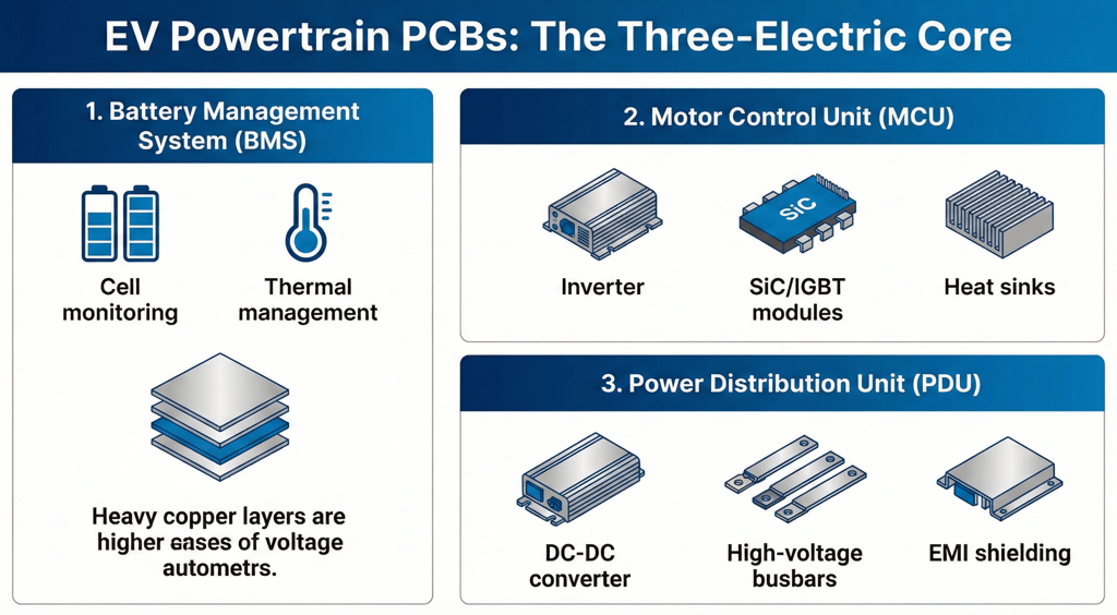
1. Battery Management Systems
Every single cell's voltage gets watched by the BMS, like a quiet watcher keeping tabs on numbers. Instead of just tracking power levels, it also checks how much life remains in the battery overall. While most systems ignore wear, this one measures aging too - silently counting each sign of fatigue.
A single volt here can throw everything off. Sitting high on a stack that pushes 400V up to 800V, the system still needs to catch changes in tiny fractions - mere thousandths of a volt. One wrong reading and stability slips. Accuracy holds tight only when isolation is absolute. Without clean separation, noise creeps in, distorting every small signal beneath.
Twisting through tight spaces inside battery setups, these circuits mix stiff and bendy parts. Where brains are needed - like ASIC chips - thick stacked layers take charge. Instead of heavy wire bundles, thin flexible links stretch between them, cutting down both mass and weak spots. Fewer connections mean fewer things that can go wrong.
2. Motor Control Unit Inverter
Power from the battery goes to the MCU, which turns it into spinning current for the motor. When slowing down, that same unit captures energy instead of losing it.
High heat plus intense current now push limits. As companies adopt silicon carbide mosfets for better performance, speed and compact design surge forward. Still, stress builds fast under such tight conditions.
Finding space on a circuit board? Regular fiberglass won’t cut it. Thick copper layers - six ounces thick or even heavier - step in when heat needs moving, not blocking. So do special ceramic bases where copper sticks directly, helping spread warmth fast.
3. Vehicle Control Unit and Onboard Charger
A single unit handles how much twist goes to the wheels, whereas charging duties fall to another part when plugged in. Power moves from wall to storage under one system's watch, at the same time a different brain adjusts push strength across axles.
Putting pieces together gets harder when everything packs into one unit. Designs shift toward combining parts, making space tight on circuit boards. Squeezing components closer happens, yet they still need safe gaps between them electrically. More stuff in less room pushes limits of how things fit and keep working.
Material Science Moving Past Standard FR4
Heavy price tags usually shape what stuff is made of when it comes to gadgets. When a circuit board inside an electric vehicle breaks down - peeling apart, burning up, or growing tiny metal threads - it might spark dangerous overheating. That kind of meltdown pushes engineers to dig deep into heat science before picking any part material.
High Tg And CtI Ratings
Softening kicks in once epoxy hits its glass transition mark. Usually above 170°C, that threshold sets the standard for drivetrain uses. When it comes to electric vehicles with strong voltage demands though, another measure matters far more - CTI takes center stage.
When electric vehicles shift from 400-volt to 800-volt systems for quicker charging, sparks jumping along circuit boards become more likely. Resistance to leakage paths shows up clearly in materials rated CTI Level 0 or 1 - those handle over 600 volts without breaking down. Because moisture and dirt can create hidden trails, automakers aiming for durability tend to choose halogen-free layers that resist tracking. Over a car’s lifetime, which may stretch fifteen years, insulation failure could start small but grow serious - better materials help avoid that. Reliability under stress matters most where voltage climbs and conditions turn damp.
The Rise of Ceramic and Metal Core PCBs
Heat builds up fast in inverters when using standard circuit board materials. Because IGBTs or silicon carbide parts pump out so much warmth, regular FR4 can’t move it away quickly enough. Most organic setups struggle past certain temperature points. What you need is material that handles heat better than 0.3 watts per meter-kelvin. Without that, things get too hot to run safely.
Starting off with a copper foil on top, these boards stack a slim insulating film below it, then cap things with a solid slab of aluminum or sometimes copper. Thermal performance lands between 1 and 3 watts per meter-kelvin - enough to handle heat in onboard chargers. Instead of complex layers, they keep cooling straightforward. That range works well inside power parts like DC-to-DC boxes. Built tough, their design channels warmth down through the base plate fast.
When it comes to high-performance traction inverters, materials like Alumina or Silicon Nitride form the base. Thick copper layers attach straight onto these ceramics through a process known as Direct Bonded Copper. Thermal performance reaches about 24 watts per meter-kelvin with Alumina. With Silicon Nitride, that number jumps close to 90. Heat moves efficiently thanks to the strong bond between metal and insulating layer. Each material suits applications where cooling matters just as much as electrical isolation.
The Manufacturing Gauntlet Facing Electronics Assembly
A solid PCB layout means little without proper execution. What happens next - placing tiny parts by machine, then building the whole unit - brings fresh challenges for contract manufacturers.
Avoiding Gaps in Solder Connections
Inside power electronics, solder isn’t just for sticking parts together - it moves heat too. Trapped air inside that solder layer? It blocks warmth like a blanket. When a MOSFET can’t dump excess heat into the board, things go wrong fast. Too much buildup means the chip runs hotter than it should - failure follows quietly.
Tough rules like IPC-A-610 Class 3 apply to cars, yet electric drivetrains usually demand even more. Top production methods, including ones from Ominipcba, rely on vacuum reflow when joining parts. As solder melts, pressure drops sharply, pulling out trapped air. This step slashes empty pockets under components, keeping levels beneath five percent. Less than that number matters most when heat must move fast through powerful circuits.
Heavy copper etching lamination
Heavy copper circuit boards need a particular kind of chemical treatment during fabrication. When typical alkaline solutions are used, they sometimes eat away at metal hidden under protective layers. This erosion happens below the surface, where the coating fails to shield the material fully. As a result, connections may lose grip on the base material over time.
Pressing the heavy copper sheets together needs strong force so the sticky resin can reach every space under the bulky tracks. When there is not enough goop squeezed in, empty pockets form. These hollow spots tend to crack apart when heat changes happen.
Cleanliness and Ionic Contamination
When dust with salts sticks around in high-voltage DC paths, tiny metal bits start moving if voltage is on. Voltage pushes these particles from one path to another. Over time, they grow tree-like branches. Those strands connect points they should not. A bridge forms where current jumps across, leading to failure.
Something called Conductive Anodic Filament growth sneaks through electric vehicles like an unseen threat. Instead of waiting, modern electronic manufacturing steps up with strong cleaning routines, backed by Ion Chromatography checks that go well beyond what regular products need. It is not about looking clean - it is about staying chemically balanced at a deep level.
Keeping Signals Clear Despite Nearby Noise
Inside the electric vehicle's drive system, strong magnetic disturbances are common. When large electrical flows shift inside the inverter, they send out powerful waves of interference. Even so, the battery monitoring unit and vehicle control system need to pass sensitive information only a short distance from those noisy zones.
Differential Signaling with Isolation
When signals travel across a circuit board, some paths need special handling. Instead of running wires close together, they’re spaced just right so interference cancels out - this helps with data lines like those in vehicle networks or isolated digital links. What really matters, though, isn’t just how traces are paired but where everything sits on the board. Areas carrying strong power live far from delicate circuits, separated by gaps cut straight into the material itself - the empty space acts like a wall against unwanted voltage jumps.
When building complete circuit boards, keeping space between parts matters a lot. How well the protective coating lines up affects how the board works, not only how it looks. A slight misalignment of that layer could uncover metal where voltage needs room to breathe, putting the whole unit's safety at risk.
Reliability Testing The Burn In
A machine emerges not by chance but through trial. Last steps in making circuit boards demand extreme tests against heat, cold, vibration. Survival here means readiness for real-world chaos.
Temperature Changes and Sudden Shifts
One moment it's freezing near the Arctic, next it's blazing under desert sun - vehicles face both extremes fast. Inside them, circuit boards get pushed through sudden swings: from deep cold at minus forty to scorching heat past one hundred twenty-five degrees Celsius. These shifts challenge how differently copper, board material, and parts grow or shrink when heated or cooled.
Cracking tends to be the main issue in these cases. When the board grows thicker, tension builds on the copper lining inside a plated hole. This lining might snap if it lacks enough thickness or flexibility, breaking the connection. To reduce risk, makers such as Ominipcba apply tight rules on how thick the coating must be - typically more than 25 micrometers for high-reliability uses - and pick materials that swell less across the thickness. Instead of growing much when heated, the resin stays stable.
Vibration and Mechanical Stress
Every now and then, you notice how different an EV sounds compared to older engine types - sharp hums instead of deep growls. Those noises come from the motor spinning fast, along with feedback from tires meeting pavement. Inside the electronics, big parts such as capacitors need more than tiny metal welds to stay put. They rely on goopy sealants poured around them or thin layers squeezed underneath. Putting that gunk in place takes care - one dab too small won’t hold anything, yet a blob too wide might crack connections when heat makes things swell.
Integrated powertrain shaping future vehicle design
Nowhere is change faster than in how parts get packed together - motor, inverter, gearbox, sometimes even OBC squeezed into one housing. Weight drops when things merge like that, wires vanish too. Heat builds up more though, tucked in tight. Space gains come at the cost of cooling headaches.
Now shaping up, PCB tech moves into deeper complexity. Inside layers, power parts tuck neatly - cutting unwanted electrical noise before it starts. Not just stacking more layers, but building smarter ones changes how things fit together. Higher voltage needs tougher insulation; think 800 volts climbing toward a thousand. Materials must hold strong without bulking up the design. Thin stays thin, yet handles surges better than older versions ever did.
Conclusion
Nowhere else does circuit board building matter more than in electric vehicle drivetrains - it has become central to how cars are engineered today. Instead of just putting parts together, it blends high-end materials work with exacting pattern carving, pressure-controlled mounting steps, then meticulous inspection down to the smallest flaw.
Getting ahead here needs more than equipment - it takes an EMS provider who grasps how things break. Not just filling gaps during SiC module soldering but hitting spotless ion levels on BMS boards matters most. Ominipcba shows what counts: building tough electronics right, every time. That reliability? It shapes everything coming next in electric tech.
Related Articles
Contacts
Email: sales@ominipcba.com
Mobile: +86-185-7640-5228
Copyright © 2007-2026. Omini Electronics Limited. All rights reserved.
Head Office: +86-755-2357-1819
Services
Your China turnkey partner for electronics manufacturing. We bridge design to delivery by leveraging the Shenzhen electronics ecosystem for precision engineering and streamlined PCBA supply chain logistics.
Ready to Build?
Get a comprehensive quote within 24 hours.
