Phone: +86-755-2357-1819 Mobile: +86-185-7640-5228 Email: sales@ominipcba.com whatsapp: +8618576405228

From Schematic to Shelf: An Ultimate Guide to the Electronics Manufacturing Process
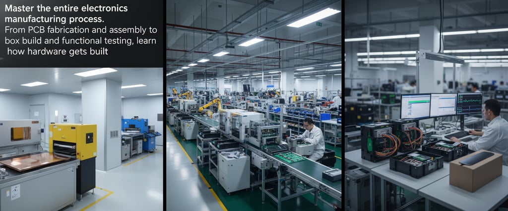
Master the entire electronics manufacturing process. From PCB fabrication and assembly to box build and functional testing, learn how hardware gets built
PCB MATERIALS
Amanda
2/5/20253 min read
For hardware engineers and procurement managers, a product launch is defined by critical milestones: design freeze, prototyping, pilot runs, and mass production. However, bridging the gap between a CAD file and a physical device requires navigating a complex ecosystem of chemistry, physics, and precision logistics.
As the Electronics Manufacturing Services (EMS) market expands—driven by IoT, automotive electronics, and industrial automation—the quality of your hardware depends on the integrity of your manufacturing partner. Whether you are outsourcing to an EMS provider or overseeing a production line, here is the professional breakdown of how raw materials transform into functional hardware.
1. Electronics Design and Engineering for Manufacturability (DFM)
The foundation of a successful build is laid long before the machines start running. Professional electronic design is about creating a blueprint optimized for the factory floor.
Using industry-standard CAD software, engineers generate the essential documentation:
Schematics: The logical map of electrical connections.
PCB Layout: The physical routing of copper traces and component footprints.
Gerber Files & ODB++: The universal fabrication data that tells the factory where to etch, drill, and apply solder mask.
Pro Tip: Integrating DFM (Design for Manufacturability) best practices at this stage—such as optimizing thermal relief and component spacing—prevents costly redesigns and improves production yield.
2. PCB Fabrication: Creating the Substrate
Once the design is finalized, the bare board (substrate) is manufactured through a high-precision chemical and mechanical process.
Etching: Unwanted copper is chemically removed from the core material (typically FR-4), leaving behind the precise trace patterns required for the circuit.
Drilling & Plating: Mechanical or laser drills create vias to link layers. These holes are then electroplated with copper to ensure electrical continuity.
Solder Mask & Silkscreen: A polymer coating protects traces from oxidation and bridges. Finally, the silkscreen layer is printed to provide component designators (e.g., R1, C1) for assembly.
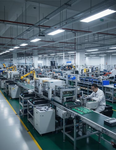
3. PCB Assembly (PCBA)
This is the stage where the bare board becomes a functional system.
Solder Paste Printing: High-precision stencils deposit solder paste onto the SMD pads.
High-Speed Pick-and-Place: Robotic mounters pick components from reels and place them onto the board with micron-level accuracy.
Reflow Soldering: The assembly passes through a multi-zone reflow oven, melting the paste to create permanent mechanical and electrical joints.
SMT vs. Through-Hole Technology:
While Surface Mount Technology (SMT) is the standard for high-density modern electronics, Through-Hole Technology (THT) remains essential for connectors and high-power components that require superior mechanical strength via wave soldering.
4. Quality Control and Inspection
To achieve zero-defect manufacturing, rigorous inspection protocols are non-negotiable.
AOI (Automated Optical Inspection): High-speed cameras and AI algorithms compare the board against a "Golden Sample" to detect placement errors, polarity issues, or solder bridges.
X-Ray Inspection: Vital for BGA (Ball Grid Array) and QFN packages. X-ray allows technicians to inspect hidden solder joints for voids or shorts that optical cameras cannot see.
5. Functional Testing (FCT)
While inspection checks for assembly accuracy, testing verifies performance.
ICT (In-Circuit Testing): A "bed of nails" fixture tests individual components for resistance, capacitance, and shorts. This is the gold standard for high-volume production.
Flying Probe Testing: Using robotic probes, this method requires no custom fixtures, making it the most cost-effective solution for PCB prototyping and small batches.
6. IC Programming and Box Build Assembly
After the PCBA is verified, the "intelligence" is added. IC Programming involves flashing firmware or bootloaders onto microcontrollers.
The process culminates in Box Build Assembly, where the PCBA is integrated into its final enclosure. This includes cable harness routing, display integration, and mechanical fastening. Every unit undergoes Final Functional Testing (FCT) to simulate real-world usage before shipment.
Partner with OminiPCBA for Seamless Manufacturing
The journey from a design file to a market-ready product is filled with technical nuances. At OminiPCBA, we simplify the electronics manufacturing process for you.
From BOM optimization and DFM analysis to complex rigid-flex assemblies and full box builds, we serve as your strategic manufacturing partner. Let our expertise in fabrication and assembly handle the details so you can focus on innovation.
Related Articles
Contacts
Email: sales@ominipcba.com
Mobile: +86-185-7640-5228
Copyright © 2007-2026. Omini Electronics Limited. All rights reserved.
Head Office: +86-755-2357-1819
Services
Your China turnkey partner for electronics manufacturing. We bridge design to delivery by leveraging the Shenzhen electronics ecosystem for precision engineering and streamlined PCBA supply chain logistics.
Ready to Build?
Get a comprehensive quote within 24 hours.
