Phone: +86-755-2357-1819 Mobile: +86-185-7640-5228 Email: sales@ominipcba.com whatsapp: +8618576405228

mSAP Technology: Redefining Ultra-Fine Pitch PCB Fabrication
Break the 30µm trace width barrier. Discover how the Modified Semi-Additive Process (mSAP) overcomes subtractive etching limitations to enable next-gen HDI and SLP electronics.
PCB TECHNOLOGYPCB MANUFACTURINGPCB ASSEMBLY
OminiPCBA
1/8/20267 min read
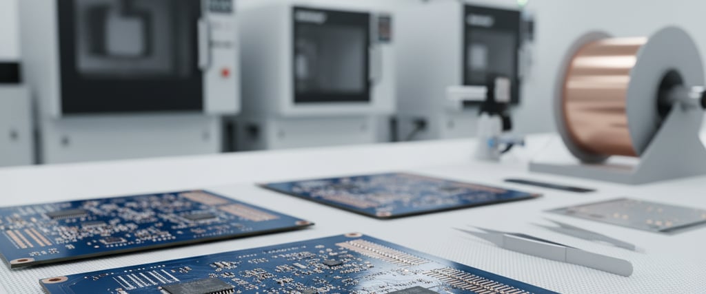
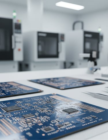
Shrinking gadgets like phones and fitness trackers keeps pushing how small circuit boards can get. Making circuits used to mean removing copper to form paths that carry signals. As lines on boards grow finer than 40 micrometers, though, old techniques fall short. Chemical etching eats sideways, leaving uneven edges that distort shapes. Those sloped sides mess up performance while using more space than needed.
Out steps the Modified Semi-Additive Process - mSAP. Born in chip substrate work, it slipped into premium PCB making, linking regular boards with silicon-level design. It doesn’t tweak old ways - it flips how traces take shape. Rather than etch away copper to reveal paths, firms build lines upward inside a template, forming what we see as Substrate-Like PCBs. These underpin top-tier smartphones now. The shift feels quiet - but runs deep.
The Shape of Missing Parts
Understanding why mSAP matters starts with seeing how old methods fall short. Instead of building up, traditional ways begin with too much copper stuck onto an insulating base - usually between 12 and 35 microns thick. Light-sensitive material shapes the design on top. Then comes a wash that strips away uncovered metal. Trouble appears because the solution doesn’t just dig down - it spreads out. That sideways bite blurs fine lines.
This lateral erosion creates a "etch factor," resulting in traces with wide bases and narrow tops. When the target line width drops to 30µm, this trapezoidal shape becomes disastrous. The electrical impedance fluctuates uncontrollably along the trace, and the wide footing prevents tighter spacing between adjacent lines. Furthermore, the variation in copper density makes maintaining a consistent 50-ohm impedance nearly impossible for high-speed interfaces.
Instead of thick copper, mSAP begins with a film just 2 or 3 micrometers wide. That thin sheet isn’t meant to carry current - it only helps build up metal through plating. Because it starts so slim, stripping away leftover copper later takes much less time. Less exposure means edges stay sharp, avoiding sideways erosion under traces. Traces end up almost perfectly square in shape, packing more conducting space into each line. Tight gaps down to 20 microns become possible without sacrificing performance.
The Big Change in Making Tiny Circuits
Switching to mSAP means rebuilding how imaging works from the ground up. Not enough detail comes through when using old-style film exposure for such tiny patterns. Most factories producing electronics with mSAP have turned entirely to Laser Direct Imaging instead. Here, the dry film resist acts differently - almost backwards compared to older etching methods.
Where copper needs protection during subtractive etching, the resist forms a shield. Instead, in mSAP processes, uncovered spots mark where metal stays. Light from a laser draws what comes next - flipping visibility: dark becomes path. These carved paths later host conductive lines. Think of the plating resist like a stencil shaped with care. How fine the LDI can focus decides how clean those tiny grooves turn out. Sharp details emerge only if the exposure tool delivers clarity.
It's about how tall something is compared to how wide. When paths shrink sideways, the gaps above them grow longer from top to bottom. Getting liquid to move fresh material deep into those tiny trenches tests what fluids can do under pressure. Stuck pools mean less copper reaches the base, which risks empty spots or uneven layers. Modern setups rely on upright tanks where jets blast chemical mix straight down into narrow openings, keeping flow steady even in tight spaces.
Electrolytic Growth and Material Science
Bottom up, copper begins to climb through the tiny pathways after the shape is set. With power moving across the initial coating, charged particles are pulled into open grooves. Filling happens slowly, driven by electrical pull rather than pouring. Growth sticks close to the base at first, rising only as space allows. What builds isn’t poured metal but layered buildup guided by current.
Right now, metal qualities matter a lot. Instead of spreading sideways, the copper that plates on surfaces usually grows upward. Unlike regular annealed copper sheets, its tiny crystal pattern lines up differently. When bending is involved or sudden heat changes happen, this alignment needs careful handling. Chemicals added into the liquid where plating occurs - such as smoothing agents, shine enhancers, and support molecules - influence how copper bits form and stack. These substances guide the way microscopic pieces come together during buildup.
What holds the copper to the base matters a lot here. In regular circuit boards, tiny bumps grab hold like sandpaper. High-speed designs skip those bumps to cut signal drag. Smooth surfaces mean glue-like bonds take over instead of texture. Special gas zaps or molecular primers step in to lock things together. Without these tricks, heat changes could peel layers apart slowly. A single gap might spread until connections fail down the line.
The Flash Etch Precision Subtraction
Once plating reaches the right thickness, workers take off the resist coating. Left behind sits the fresh circuit resting above the initial thin seed film. Next comes flash etching - also called selective removal. Its job? Clearing out that 2-micron seed layer between lines while leaving the new copper untouched.
Since the plated copper is significantly thicker (e.g., 20µm) than the seed layer (2µm), the etchant removes the seed layer quickly before it can significantly erode the main conductor. However, even this brief exposure can cause minor pitting or surface roughness. Process engineers must balance etchant aggression with inhibitor chemistry to protect the sidewalls of the traces. This step defines the final insulation resistance and breakdown voltage between lines; if the seed layer is not completely cleared, micro-shorts (dendritic growth) can occur over time.
Effects on PCB Assembly and SMT
Making changes with mSAP shifts how PCBs are put together later on. Because the base board is more accurate, pads can be much tinier - opening space for 008004-sized parts. Tiny spacing also supports BGAs packed tighter than 0.35 millimeters apart.
Smaller sizes in the SMT process demand tighter control over how solder paste is applied. Because mSAP board openings are extremely tiny, getting paste out cleanly depends heavily on hole depth compared to width plus the fineness of metal particles used. As things shrink, finer powders - like Type 5 or even Type 6 - are now more common just to keep deposit amounts stable. Oddly enough, it's the shape of the pads that helps: their rectangle form gives parts a level base when placed, which in turn keeps small components from lifting at one end during heating.
Flatness tends to suffer because the board lacks flexibility. Since mSAP goes into slim, dense HDI setups, bending shows up when heat hits during reflow. To keep things level while moving through the oven, turnkey PCBA suppliers lean on custom supports or trays. Heat absorption by those tools changes how the profile works - adjustments keep solder flow smooth without frying delicate parts.
Signal Quality and Electrical Behavior
Every now and then, signals move faster than expected across tiny pathways. Because of how electricity behaves at high speeds, the outside layer of a wire ends up doing most of the work. When frequencies climb, electrons stick to the surface, avoiding the core. That behavior means texture matters more than ever. Rough edges slow things down without warning.
Bumpy textures on regular copper help it stick to insulating layers, yet that uneven surface boosts electrical loss when signals race into the GHz range. Through mSAP, thinner or ultra-thin foils serve as the starting point instead. Smoothness becomes possible during plating, shaping copper almost glasslike under precise control. Instead of jagged edges, clean right-angle walls form between traces - this steadies how electric fields link across paired lines. Such consistency keeps signal resistance tightly within narrow margins, exactly what high-speed standards such as PCIe Gen 5/6 and 112G SerDes demand.
When Ominipcba checked reference setups, they found channels made with mSAP technology lose less signal over distance than traditional ones. This happens because mSAP shapes conductors more evenly while keeping surfaces smoother. Same-length paths behave differently when built this way. Geometry plays a big role here - tighter control means fewer disruptions along the line.
Cost Factors and Production Output
Despite its technical superiority, mSAP is not a universal replacement for subtractive etching due to cost. The capital investment for LDI machines, specialized plating lines, and automated optical inspection (AOI) systems capable of resolving sub-30µm features is substantial.
It takes more time too. Instead of just printing and etching, there are extra stages like chemical plating, applying protective film, electrically building up metal layers, removing coatings, then thin etching - each one adding complexity. What really pushes up costs is how many panels get lost along the way. If even a speck of dust shows up when imaging happens, or if tiny gaps form while depositing copper, that whole expensive board might be unusable. Because of this, only tightly packed circuit designs go through mSAP - usually found in phones, top-tier watches, and compact chip packages where saving space matters most.
The Future Moves from mSAP to SAP
As line widths approach 10µm to 15µm, even the thin seed layer of mSAP becomes a liability. The industry is gradually moving toward pure Semi-Additive Processing (SAP), where the dielectric is built up without any initial copper foil. Instead, a catalyst is applied directly to the resin, and electroless copper forms the seed layer entirely chemically.
One step forward means electronics making looks more like chip packing. Closer teamwork becomes necessary - material makers must align with machine builders, especially on resins that allow chemical plating minus surface scraping. That shift changes how parts come together.
Conclusion
A new step in circuit board making has quietly changed how things work. Not just connecting parts anymore, the board now acts more like the chips it holds. Because of this shift, tighter spaces and better speed became possible where they could not be before. Precision grew sharper when methods evolved beyond old limits. What once seemed too fine to build is now within reach through careful changes. The path forward opened up without fanfare or drama.
Still, using this tech means seeing how everything connects across production. Not just picking ultra-pure insulating materials but also fine-tuning the full circuit board heating process - each step shifts once measurements dive into single-digit microns. With more speed needed in less space, mSAP won’t stay rare; it’ll become normal for top-tier devices, pushing suppliers at every stage to sharpen their accuracy.
Related Articles
Contacts
Email: sales@ominipcba.com
Mobile: +86-185-7640-5228
Copyright © 2007-2026. Omini Electronics Limited. All rights reserved.
Head Office: +86-755-2357-1819
Services
Your China turnkey partner for electronics manufacturing. We bridge design to delivery by leveraging the Shenzhen electronics ecosystem for precision engineering and streamlined PCBA supply chain logistics.
Ready to Build?
Get a comprehensive quote within 24 hours.
