Phone: +86-755-2357-1819 Mobile: +86-185-7640-5228 Email: sales@ominipcba.com whatsapp: +8618576405228

Optical PCB & Silicon Photonics: The Future of High-Speed Interconnects
Break the bandwidth bottleneck. Analyze the integration of Silicon Photonics with printed circuit boards, covering embedded waveguides, CPO assembly, and sub-micron manufacturing challenges.
PCB TECHNOLOGYPCB MANUFACTURINGPCB ASSEMBLY
OminiPCBA
1/1/20263 min read
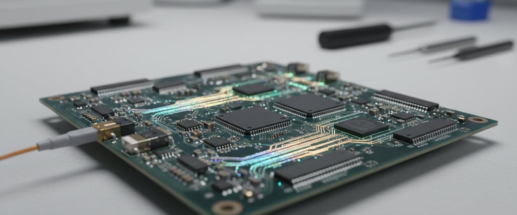
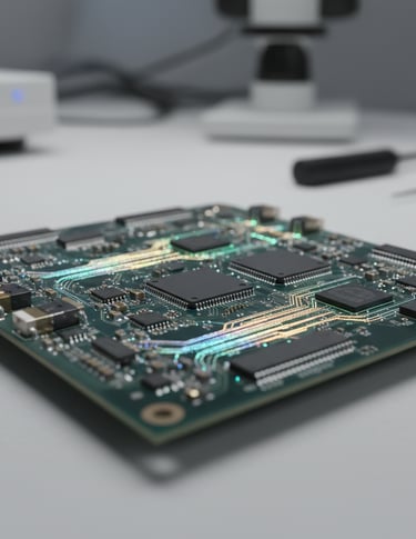
In the era of 224 Gbps per lane, traditional copper traces are hitting a physical ceiling. As data centers demand unprecedented bandwidth, the electrical resistance in copper leads to significant signal degradation and excessive heat generation. Even over short distances, signal integrity falters, requiring power-hungry retimers to compensate. To meet the "Petabit hunger" of next-generation AI and computing, the industry is shifting toward Electro-Optical Circuit Boards (EOCB).
By integrating Silicon Photonics directly into the PCB substrate, engineers are replacing electrons with photons. This transition eliminates electromagnetic interference (EMI) and thermal bottlenecks, allowing light to transmit data across chips with near-zero latency and minimal power consumption.
Overcoming the "Copper Wall"
The move to Optical PCBs is driven by the fundamental limitations of electrical physics. A high-end copper trace using Megtron 7 material struggles to maintain an 112G PAM4 signal beyond 10 inches before it dissipates into noise.
In contrast, embedded optical waveguides offer a paradigm shift in performance:
Low Attenuation: Optical channels lose only approximately 0.05 dB/cm, significantly outperforming copper at high frequencies.
EMI Immunity: Light-based signals are immune to magnetic noise, eliminating the need for bulky shielding or wide trace spacing.
Energy Efficiency: Photonic links utilize a fraction of the energy required by copper, preventing the thermal runaway common in high-density server environments.
Optical PCB Structure and Materials
An Optical PCB is more than a standard board with fiber attachments; it is a complex hybrid utilizing built-in light pathways.
Polymer vs. Glass Waveguides
The choice of waveguide material dictates the PCBA manufacturing process:
Optical Polymers: These are the industry standard for board-level integration due to their compatibility with standard lamination and lithography processes. They can withstand lead-free soldering temperatures up to 260°C.
Glass Waveguides: Thin glass layers offer superior optical transparency and minimal signal loss. However, their brittleness and Coefficient of Thermal Expansion (CTE) mismatch with organic substrates pose significant challenges during thermal cycling.
Co-Packaged Optics (CPO): The System Enabler
Co-Packaged Optics (CPO) is the primary catalyst for Optical PCB adoption. By moving the optical engine off the edge of the board (traditional pluggables like QSFP-DD) and placing it directly adjacent to the ASIC, the electrical "reach" is minimized.
This proximity reduces power consumption and removes the bandwidth bottlenecks found in traditional layouts. As a result, the PCB must now function as a dual-medium platform, routing both high-speed light signals and traditional electrical power.
Sub-Micron Precision: The Alignment Challenge
Unlike electrical components, which benefit from the self-aligning properties of surface tension during reflow, optical components demand sub-micron precision. Aligning a laser to a 9μm single-mode waveguide requires an accuracy of 0.5μm to 1.0μm.
To achieve this, advanced PCBA facilities utilize Active Alignment technology:
Real-Time Feedback: The laser is powered on during placement.
6-Axis Adjustment: Robotic systems adjust X, Y, Z, Tilt, Yaw, and Roll.
Optimization: The component is locked into place only when peak signal coupling is detected.
UV Curing: Specialized adhesives are cured instantly with ultraviolet light to "freeze" the alignment.
Data from OmniPCBA indicates that switching from passive to active alignment can improve signal coupling by 3dB—effectively doubling the usable light signal.
Optical Vias and Thermal Management
Directing light vertically between board layers requires 90-degree optical vias and 45-degree turning mirrors. These mirrors are micro-machined and often coated with gold or aluminum to maximize reflectivity. Maintaining the structural integrity of these mirrors during high-pressure lamination is critical to preventing signal loss.
Furthermore, while photons do not generate heat, the laser diodes are highly temperature-sensitive. Thermal shifts can cause wavelength drifting in WDM (Wavelength Division Multiplexing) systems. Advanced EOCBs incorporate copper heat sinks or active cooling modules directly beneath the photonic engine to ensure wavelength stability.
Manufacturing Excellence: Cleanliness and Reliability
In the world of Optical PCBA, a 5-micron dust particle is a catastrophic failure point, not just a minor defect. Manufacturing must occur in Class 100 to Class 1000 cleanrooms.
Surface Preparation: Plasma treatment is used to remove organic contaminants at the molecular level.
Advanced Cleaning: Standard aqueous washes are replaced by CO2 snow sprays or specialized solvent vapor baths to ensure lens surfaces are pristine.
Long-Term Reliability: Optical polymers are tested for "yellowing" (UV degradation) and moisture absorption, which can interfere with 1310nm and 1550nm telecom wavelengths.
The Rework Paradox
High-value Optical PCBs present a "zero-defect" challenge. Because components are UV-bonded rather than soldered, rework is extremely difficult. OmniPCBA emphasizes a "Shift Left" quality strategy: implementing OTDR (Optical Time-Domain Reflectometry) testing on individual waveguides before final assembly to maximize yield and minimize the loss of expensive substrates.
Conclusion: The Photonic Era
The convergence of semiconductor lithography and traditional PCB manufacturing marks the beginning of the Photonic Era. As copper reaches its physical limits, the ability to manufacture hybrid electronic-light systems will define the next generation of supercomputing and AI infrastructure. OmniPCBA remains at the forefront of this evolution, mastering the precision required to turn light into data.
Related Articles
Contacts
Email: sales@ominipcba.com
Mobile: +86-185-7640-5228
Copyright © 2007-2026. Omini Electronics Limited. All rights reserved.
Head Office: +86-755-2357-1819
Services
Your China turnkey partner for electronics manufacturing. We bridge design to delivery by leveraging the Shenzhen electronics ecosystem for precision engineering and streamlined PCBA supply chain logistics.
Ready to Build?
Get a comprehensive quote within 24 hours.
