Phone: +86-755-2357-1819 Mobile: +86-185-7640-5228 Email: sales@ominipcba.com whatsapp: +8618576405228

PCB Interior Architecture: The Engineering of Embedded Passives
Maximize PCB density and minimize parasitic inductance by embedding resistors and capacitors. deeply analyze the fabrication logic, signal integrity gains, and the "zero-rework" reality.
PCB TECHNOLOGYPCB MANUFACTURINGPCB ASSEMBLY
OminiPCBA
1/2/20267 min read
Hills and valleys of a circuit board used to follow a clear rule: parts up front, wires behind. That flat layout worked well - until it did not. Speeds now sprint beyond 56 Gbps, gadgets squeeze down to patches worn on skin. Hidden drag inside tiny solder points and holes resists progress. A fix emerges only when small elements dive below the surface, buried within the base layer instead.
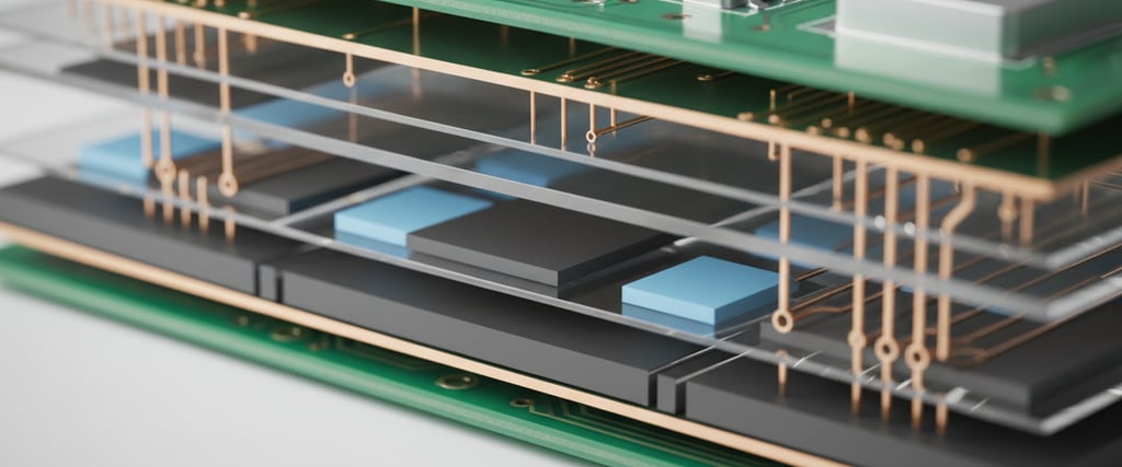
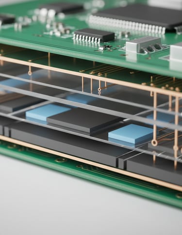
Hidden parts inside circuits do more than shrink size - they clean up electric flow. Placing resistors and capacitors deep within layer stacks removes height gaps from power supply to device, which sharply cuts loop resistance wrecking fast power systems. That shift pulls chip making and base materials closer together, making it hard to tell where the circuit board stops and the build starts.
The Physics of Proximity Why Hide Parts Inside?
Figuring out why embedding matters starts by measuring regular surface mount costs. A small 0402 cap placed up top needs pads, routing paths, then holes through layers just to reach inner power sheets. Even when routed neatly, that setup adds around 500 to 800 picohenries of inductance. Below certain speeds, it makes little difference. Above a few billion cycles per second though, that hidden coil effect blocks fast current bursts - so the chip starves during sudden power spikes.
Putting capacitance right under the chip skips both solder points and tiny vertical links. With the storage component sitting just beneath the main part, electrical loops shrink so much that inductance drops below 100 picohenries. Because space gets used smarter, power lines stay steadier and noisy swings fade out - meaning fewer support capacitors show up on the parts list.
Thin Film Embedded Resistors
Not every resistor stays separate. Some slip right into the board itself through a method using thin layers, which works by removing material instead of adding parts like surface mounting does. A different path entirely. Factories rely on unique copper sheets, these come dressed in materials meant to resist - think nickel mixed with chromium, or sometimes nickel paired with phosphorus. The build changes shape piece by quiet piece.
Starting with the making process, copper that carries current gets removed through etching to set where connections will end. After that, cutting into the resistive substance shapes the actual resistor part. What the total resistance turns out to be depends on how the material resists flow across its surface - called ohms per square - and also how big or small the cut region is shaped.
Fine control matters most in this step. A separate resistor gets checked first, yet one built into the board takes shape right where it belongs. Changes in how long or what mix eats away material might shift its size, nudging resistance off target. Because of this, trusted makers adjust with focused light beams. Fine-tuned by slicing through the resistive material, the beam reshapes how electricity flows, pushing resistance higher until exact specs are met. Built without solder connections, these parts withstand heavy shaking - fewer weak spots form where joins would fail.
Embedded Capacitors: Planar vs. Discrete
Split down the middle, the approach to handling capacitance leans on two separate paths - spreading it flat across surfaces or tucking small chips right inside. One builds thin layers that hold charge like sheets, while the other slips tiny storage units into tight spots within the structure. Each way keeps things running but does so by different means and placements.
Instead of adding parts, this method uses the circuit board’s layers directly. A power layer sits across from a ground layer, divided by an ultra-slim insulating sheet - usually between 8 and 24 micrometers thick. That setup turns each matched pair into a broad, flat capacitor. Materials like C-Ply boost performance; they contain nano-sized particles that increase electrical resistance inside the material. Even though one patch holds less charge than a tiny ceramic component, the effect spreads through every inch of the board. High-speed interference finds a steady path to disappear because the whole system behaves like a sponge for unwanted signals.
A single capacitor gets tucked into a hollowed-out space inside the board’s middle layers. Not only does this hold real MLCC parts, but it also supports bigger storage of charge - think microfarads instead of tiny picofarads. What makes this tough? A machine cuts the pocket first, then slips the part in before sealing everything under melted resin. After that, connections form through small holes blasted by lasers, hitting the ends of the piece exactly. Each step demands precision, since alignment can’t afford mistakes.
Hitting the mark here pushes beyond what most EMS factories handle every day. Through an epoxy coat, the laser has to find its target without seeing it - like threading a needle in the dark. A shift as small as half a human hair might leave behind either weak links or broken paths entirely.
The Zero Rework Reality
Hidden deep inside modern circuit boards, electronic parts get locked in place forever. When layers fuse together under heat and pressure, there is no way back. One tiny resistor misbehaving means nothing can be fixed later. Trapped beneath hardened resin and woven fibers, everything becomes waste. The whole unit ends up discarded without hope of repair.
Now quality checks start earlier in the process. Instead of waiting until assembly finishes, tests happen while building internal layers - especially with embedded passives. Traditional setups test at the end. But here, making sure things run smoothly shapes most of the expense. That shift changes how teams plan each step. Ominipcba found this pattern across several reviews. Though small, each inner sheet gets tested for electric flow before pressing begins. When resistance falls outside allowed limits, only that piece gets tossed - avoiding waste down the line. A single check early stops bigger losses later.
This one extra step - adding layers into a circuit board - doesn’t just raise price bit by bit. The real jump comes from how often things go wrong when more steps pile up. So engineers pick carefully which parts really need to sit inside the board. Only if saving space or improving signals outweighs the growing chance of failure do they place them deep within.
Managing Heat Below the Surface
Heat comes out of a resistor when it works. If the part sits outside, air flow carries some warmth away. But trap it under something like FR4, and the heat stays stuck. Without escape paths, one spot gets much hotter than the rest. That intense point might warp the board layering or shift resistance numbers because materials change with temperature.
Heat modeling now fits into design work like a key in a lock. Built-in parts need ways to shed warmth, so creators weave thick copper layers nearby or pack rows of small thermal holes next door. A buried resistor handles less wattage compared to one sitting on top - sometimes only half - as the stuff around it traps heat. Getting warm out proves harder when insulation wraps the part.
The Effect on SMT Assembly
One surprise shows up early on the PCB line - hidden tech makes part positioning easier but messes with material flow. Imagine a circuit board rolling into the pick-and-place station, nearly half its tiny passives already tucked in place. Fewer stops for the machine mean faster movement down the track.
A small slip can cost real money once chips are on the board. What used to be just another circuit slab now carries serious value. Mishaps during handling shift from trivial to costly fast. Temperature swings in reflow need tight control, nothing left to chance. A dropped assembly with pricey components hurts more than a blank one ever could. Already, the built-in parts went through several rounds of heating when layers were pressed together. Too much heat later on might crack them inside, especially where copper meets the part's edge. Heat history matters because weak spots grow right there.
Design for manufacturing in three dimensions
Starting mid-sentence, cavity rules come into play when embedding parts directly. Tools need real three-dimensional handling, not flat approximations. Around each tiny part, empty space stays - this gap lets goop move through during molding. Without that breathing room, bubbles sneak in where they should not be. Modeling software has to track those gaps precisely, shape by shape.
Empty spots where resin should be can cause serious trouble. When the melted resin fails to surround the whole chip while pressing, tiny air gaps stay behind. Heat from soldering makes those trapped bubbles grow - sudden splitting follows, like kernels bursting. Design reviews need to confirm paths for resin movement are wide enough, also check nearby metal layers do not block spread. A gap here pulls everything apart later.
Nowhere is timing more crucial than when designers talk to builders right at the start. Not later. The layer structure isn’t picked off a shelf anymore. Each prepreg thickness fits exactly around parts tucked inside. Precision shapes function. Details lock together before anything gets made.
Intellectual Property Meets Reliability
Hidden inside layers, circuits gain a quiet edge in safety. When key parts like resistors and capacitors vanish under ground shields, even X-rays struggle to spot them. Probing by hand? Impossible. The deeper they’re buried, the harder it gets to copy what’s there.
When it comes to lasting performance, leaving out solder joints gets rid of the weakest link in tough conditions. Instead of solder - which slowly deforms and cracks when heated and cooled repeatedly - thin-film resistors made by chemical etching hold up far better. So do copper-coated vias, which bond more securely at the metal level. These connections laugh off shaking and sudden impacts. Because they endure so well, such designs draw strong interest in car radar setups and flight electronics. Even if making them costs more upfront, their ability to last matters much more in those fields.
The Meeting of Making and Putting Together
Now the circuit board does more than hold wires on a flat surface. Little parts live inside it, built right into its layers. That change means factories must adapt how they make these boards. Instead of just printing paths, they shape materials like chip makers do. Tools such as lasers and chemical etching work with extreme care. Precision matters as much as it does when sealing tiny silicon devices.
Right now only speed-focused projects can afford it, yet the laws behind fast signals mean everyone will have to use it sooner or later. To today’s builder, the circuit board isn’t merely a base anymore - space inside matters just as much.
Related Articles
Contacts
Email: sales@ominipcba.com
Mobile: +86-185-7640-5228
Copyright © 2007-2026. Omini Electronics Limited. All rights reserved.
Head Office: +86-755-2357-1819
Services
Your China turnkey partner for electronics manufacturing. We bridge design to delivery by leveraging the Shenzhen electronics ecosystem for precision engineering and streamlined PCBA supply chain logistics.
Ready to Build?
Get a comprehensive quote within 24 hours.
