Phone: +86-755-2357-1819 Mobile: +86-185-7640-5228 Email: sales@ominipcba.com whatsapp: +8618576405228

RF PCB Design: Bridging the Gap Between Theory and Manufacturing
Master the complexities of RF PCB design. From selecting the right stack-up to navigating the PCB manufacturing process, we cover essential tips for engineers
PCB TECHNOLOGY
OminiPCBA
12/8/20252 min read
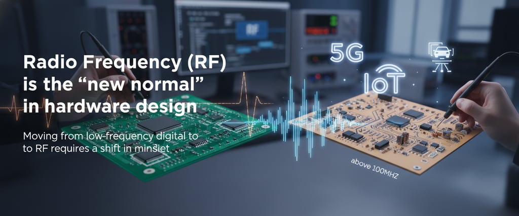
Radio Frequency (RF) technology is no longer a niche for specialized telecom. Driven by the surge in IoT, 5G, and automotive radar, RF capabilities have become a standard requirement in modern hardware. However, transitioning from low-frequency digital boards to RF designs operating above 100MHz requires a fundamental shift in engineering and procurement strategy.
At these frequencies, copper traces cease to be simple wires and begin behaving as transmission lines. For procurement managers, this means standard FR-4 stack-ups may no longer suffice. This guide explores the critical intersection of RF design theory and high-precision PCB manufacturing.
1. The Foundation: Selecting the Right Substrate
In digital design, the substrate is often just a mechanical carrier. In RF PCB manufacturing, the substrate is a functional component of the circuit.
When managing the BOM (Bill of Materials), you will find that RF laminates (such as Rogers or Arlon) carry a premium over FR-4. This cost is driven by two critical technical factors:
Dielectric Constant (Dk): RF materials offer a stable Dk across varying frequencies and temperatures. Any shift in Dk results in impedance mismatches and signal reflection.
Dissipation Factor (Df): This dictates signal loss. While FR-4 is "lossy" at high frequencies, materials like PTFE (Teflon) or ceramic-filled hydrocarbons provide a "paved track" for signals, ensuring maximum integrity.
Pro Tip: Hybrid PCB stack-ups—combining FR-4 with high-performance laminates—can optimize costs, but they require a sophisticated fabrication process to manage different thermal expansion rates.
2. RF PCB Layout Best Practices
Once the material is selected, the focus shifts to the layout. High-frequency signals are highly susceptible to skin effect losses and parasitic capacitance.
Impedance Matching: Maintaining a consistent 50-ohm environment is non-negotiable to prevent standing waves and power loss.
Precision Grounding: The return current follows the path of least inductance, typically directly beneath the signal trace. Breaking the ground plane under an RF line creates an unintended slot antenna, leading to EMI/EMC failures.
Via Management: In RF, a via acts as an inductor. Implementing via stitching (placing ground vias along copper pours) creates a Faraday cage effect, effectively isolating signals from external interference.
3. PCBA Assembly: SMT vs. Through-Hole
The impact of assembly on RF performance is profound. In the RF world, SMT (Surface Mount Technology) is the industry standard. Through-hole components have long leads that introduce parasitic inductance and act as unwanted antennas. SMT components minimize these parasitics by mounting flush to the board.
Assembly Precision: A minor misalignment of an 0402 RF inductor can detune a circuit. Furthermore, the reflow thermal profile must be meticulously managed, especially when using ceramic substrates that exhibit different thermal expansion characteristics than epoxy glass.
4. Advanced Interconnects: Rigid-Flex and HDI
Modern RF designs are increasingly compact. Rigid-flex PCBs allow antennas to be placed on flexible polyimide sections for wearables, while processing remains on the rigid section. These designs often utilize HDI (High-Density Interconnect) technology, employing blind and buried vias to eliminate "stubs" and minimize signal reflections.
Conclusion: Partner with OminiPCBA
RF PCB design is where physics, material science, and manufacturing tolerances converge. Success requires a tight feedback loop between the layout engineer and the fabrication house from day one.
Why choose OminiPCBA for your RF projects?
Navigating high-frequency materials and precision assembly shouldn't be a solo journey. At OminiPCBA, we specialize in high-performance PCB fabrication and turnkey assembly. From complex rigid-flex antenna modules to cost-effective 5G hybrid stack-ups, our engineering team provides a comprehensive DFM (Design for Manufacturing) review to ensure your board performs exactly as simulated.
Let us handle the technical complexities of your next RF build.
Related Articles
Contacts
Email: sales@ominipcba.com
Mobile: +86-185-7640-5228
Copyright © 2007-2026. Omini Electronics Limited. All rights reserved.
Head Office: +86-755-2357-1819
Services
Your China turnkey partner for electronics manufacturing. We bridge design to delivery by leveraging the Shenzhen electronics ecosystem for precision engineering and streamlined PCBA supply chain logistics.
Ready to Build?
Get a comprehensive quote within 24 hours.
