Phone: +86-755-2357-1819 Mobile: +86-185-7640-5228 Email: sales@ominipcba.com whatsapp: +8618576405228

SLP Architecture: The Convergence of PCB and Semiconductor Packaging
SLP technology bridges the gap between HDI and IC substrates. Explore how Modified Semi-Additive Processes (mSAP) and <30µm trace geometries are redefining smartphone internals.
PCB TECHNOLOGYPCB MANUFACTURINGPCB ASSEMBLY
OminiPCBA
1/4/20267 min read
Inside today's smartphones, empty space counts more than gold in tech circles. With users wanting longer battery life, advanced cameras, bigger lenses, faster wireless signals - room left for core components shrinks fast. Old-style circuit boards, built using long-standing techniques, now struggle to keep up. Those methods carve away material to form tiny pathways, but hitting marks below forty millionths of a meter gets messy. Precision fades when patterns get that fine.
To break this barrier, the industry has adopted Substrate-like PCB (SLP) technology. SLP is not merely an evolution of the printed circuit board; it is a migration of semiconductor packaging techniques into the macro world of the motherboard. By adopting the Modified Semi-Additive Process (mSAP), manufacturers can now achieve line widths and spacing (L/S) down to 30µm, with roadmaps targeting 10µm. This shift fundamentally alters the electronics production landscape, blurring the definition of where the component ends and the board begins.
The Physics of Density How HDI Got Stuck
Layer upon layer stacked up over time as the go-to fix for packing circuits tighter. Yet every extra level pushes the build taller along the vertical axis - no good when gadgets must stay paper-slim. A different path opens sideways: stuffing additional pathways within the very same footprint, stretching capacity outward instead of upward.
Picture a thin sheet of copper stuck to an insulating layer. This metal coating usually measures between twelve and eighteen micrometers. To shape circuits, workers cover it with light-sensitive film that hardens where exposed. Then comes bath time - chemicals wash away unneeded copper bits. When lines get finer than fifty micrometers, trouble starts. Liquid doesn’t just dig down - it creeps sideways too. So edges erode beneath the surface, leaving behind sloped walls like tiny mesas.
At 30µm, this trapezoidal geometry destroys signal integrity. The inconsistent cross-sectional area leads to impedance variations that are fatal for high-speed digital signals. Furthermore, the wide base limits how closely traces can be spaced, capping the maximum routing density. The industry required a method to grow copper with vertical precision rather than carving it away, leading to the adoption of mSAP in SLP fabrication.
mSap Powers Slp
A fresh approach to building circuits changes the old way entirely. Rather than laying down heavy metal first, it starts thin - just a delicate coat of copper applied by chemical plating on top of insulation material.
Light-sensitive film covers the surface, yet instead of shielding pathways like traditional methods, it leaves gaps in places meant to become circuits. From above, a laser carves out paths inside that layer where metal lines belong. Next comes a dip into liquid filled with charged particles, sparking buildup of copper exactly where openings exist. With boundaries formed by untouched coating, deposited material takes shape as sharp-edged ridges almost square when sliced sideways.
After the traces hit their target thickness, off comes the resist - then a swift flash etch clears away the slim seed coating. Because that seed layer is so incredibly thin next to the built-up trace, hardly any time passes during removal; edges stay sharp, no erosion sneaks in underneath. Thanks to this tight shape control, makers assembling electronics now manage circuits drawn at 30 by 30 micrometers line and space, squeezing heaps of connections onto chips and memory blocks while holding ground size flat.
Material Transformation Beyond FR4
With SLP tech, regular FR4 prepregs just won’t hold up - stability needs are way higher. Lining up tiny vias through ten or twelve layers leaves zero room for shift. Even slight stretching or shrinking of the material throws everything off alignment. Precision hinges on how little the substance moves during processing.
Now coming into wider use are ABF and high-Tg BT resins by makers of circuit boards. Pulled straight from chip package production, these substances carry sophisticated ceramic additives. What they do is limit how much material expands when heated. Less expansion means less strain on connections made with solder. That matters most when tiny bumps link chips face-down onto boards. During oven heating, tight control over stretch keeps joints intact. So stability under heat becomes a quiet guard against early failure.
Even small gaps between traces mean electric fields interfere more easily. Because of that, material choices matter a lot at 5G speeds. Slower signal loss happens when the insulating layer resists storing charge too strongly. That resistance - called Dk - is kept low on purpose. Less stored energy means less unwanted transfer between lines. So signals travel beside each other further before weakening. Heat and inefficiency still build up, yet not as fast when the material responds just right to high frequencies.
The Assembly Challenge SMT at the Micro Scale
The transition to SLP forces a recalibration of the Surface Mount Technology (SMT) process. The pads on an SLP board are often defined by the solder mask (SMD) and can be as small as 150µm. Printing solder paste onto these targets requires electroformed stencils with nano-coatings to ensure proper paste release.
Now here's something worth noticing - Ominipcba points out how the "area ratio" shapes how well paste transfers. It’s really about the opening size compared to the walls inside the stencil. When it comes to standard Type 4 solder powder, it usually doesn’t cut it. Smaller particles work better, so many SLP production setups turn to Type 5 or sometimes go all the way to Type 6. More tiny spheres mean a solid connection stands a real chance.
Bent? That matters. Such slim, packed boards twist when heated. Magnets or suction tools keep them steady through assembly steps. A shift smaller than a hair’s width breaks tiny connections. Miss that, and solder joints fail without warning.
Heat Control in Dense Layered Systems
Heat builds up more in tight spaces, even though smaller boards can run faster. When the layout gets compact, there’s less material to carry heat away. Tiny pathways resist electric flow more, so they warm up extra. This kind of loss grows with current squared times resistance, making things warmer still.
Heat escapes better when tiny metal columns link inner layers, acting like chimneys. Still, the insulating stuff between those layers traps warmth because it resists flow. Thick slabs of copper pressed inside help move energy away, or small round metals get tucked in place instead. These fixes make stacking sheets harder since everything must align under pressure.
Fewer air paths exist where parts pack tightly together during build. Because heat moves poorly through tiny spaces, new underfills mix in special powders that move warmth better than older types did. These upgraded blends link hotter chips to cooler surfaces more effectively than before.
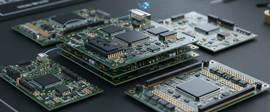
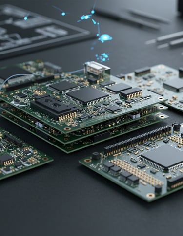
Stacked PCBs Sandwich Style
Stacked layers make room for more parts in tight spaces. A thin connector slips between two boards, pressing them together like pages in a book. This setup packs twice the tech into the same footprint. High-end gadgets use it to stay compact without losing power.
Working with this 3D setup makes building electronics tricky in new ways. Since the interposer ring links upper and lower boards, attaching it involves hidden connections. There is no way to see those joins once made. Because sight alone fails here, checking them demands X-ray scans. Without AXI, confirming solid joints would simply not happen. Fault risk climbs when gaps fill too much space inside edge connections. Should empty spots cover over one quarter of the link zone, a sudden jolt from dropping the device can snap the bond.
Inside the sandwich, heat needs time to spread fully before surfaces risk burning. Ovens using vapor phase methods handle this carefully. Nitrogen-filled convection units work too when each zone adjusts exactly on its own.
Inspection and Testing The Hidden Gap
Out in today’s compact layouts, old-school ICT just does not fit anymore. Test probes need space - space that SLPs do not offer. Trying to land on tiny 200-micron spots? That ends in harm more than help. So now teams lean into JTAG scanning, watching signals move through chip edges. Function checks take center stage too, proving circuits behave under real tasks.
Getting clear visuals during optical checks isn’t always straightforward. On certain high-speed circuit materials, the copper landing zones blend too closely with the base layer. Modern three-dimensional scanners rely on shifting light patterns to calculate how much solder paste was applied and how tall each part sits after placement, making sure vertical limits stay within range. Testing data from Ominipcba shows spotting raised connector legs - just fractions of an inch across - is something only top-tier production lines manage well.
The Economic Equation: Yield vs. Cost
Setting up mSAP and SLP needs a big financial outlay. Machines involved are LDI units, plating systems that run vertically nonstop, along with presses using vacuum lamination. Because electroless plus electrolytic plating moves slowly, processing takes more time compared to traditional subtractive etching.
What you get out matters most when calculating costs. A flaw in traditional methods could mean fixing it later or tossing the board after little work went into it. With SLP, tiny lines make things fragile - one speck of dust while imaging may break the connection completely. Since these boards stack many layers and use pricey components, throwing one away hits hard financially.
Fixing flaws early helps makers cut waste. Lasers zap tiny faults. Some machines add material where connections fail. These fixes happen inside layers, before sealing them together. Without such steps, costs climb too high. Affordable gadgets need these smart adjustments. Profit margins depend on precision tools working quietly behind the scenes.
Below 20 Micrometers Ahead
Where SLP goes next is obvious. Chasing the shape of the silicon chip keeps driving it forward. Next up, lines and spaces shrink to fifteen microns each. That tight spacing means copper's texture matters more than ever. Skin effect makes rough surfaces costlier for signals. Tiny peaks and valleys start eating into performance.
Freed-up surface room could go to bigger batteries or sensors once future versions of SLP tuck passive parts like capacitors deep into the board layers. Inside these smart substrates, raw chips might land directly during production, skipping separate packaging steps. Wire bonds may form right alongside regular pick-and-place routines on the line. Merging semiconductor finishing with standard circuit board work blurs old boundaries between contract manufacturing fields. What used to stay split now overlaps where electronics get built.
Conclusion
What once felt like a ceiling in phone design has quietly shattered. Engineers now sidestep old constraints tied to how circuits are carved, thanks to a fresh approach on the board level. This isn’t just another tweak - it reshapes what compact tech can do. Tiny pathways form more freely, boosting both space use and speed. Since smartphones arrived, nothing has bent the rules quite like this.
Still, SLP does not fit right into existing setups. Rewiring the entire supply chain becomes necessary when adopting it. Instead of just adjusting machines, each stage - from mSAP production lines to exact PCBA assembly zones - must operate within stricter margins and purer conditions. When this method spreads beyond high-end smartphones into average-priced gadgets and car electronics, handling its complex build process well could decide which companies shape future hardware advances.
Related Articles
Contacts
Email: sales@ominipcba.com
Mobile: +86-185-7640-5228
Copyright © 2007-2026. Omini Electronics Limited. All rights reserved.
Head Office: +86-755-2357-1819
Services
Your China turnkey partner for electronics manufacturing. We bridge design to delivery by leveraging the Shenzhen electronics ecosystem for precision engineering and streamlined PCBA supply chain logistics.
Ready to Build?
Get a comprehensive quote within 24 hours.
