Phone: +86-755-2357-1819 Mobile: +86-185-7640-5228 Email: sales@ominipcba.com whatsapp: +8618576405228

SMT PCB Assembly: Core of Modern Electronics
Dive into SMT PCB assembly, the backbone of modern electronics. Understand its process, benefits, and challenges, and how expert manufacturers ensure quality and efficiency.
PCB ASSEMBLY
OminiPCBA
12/21/20259 min read
Tiny parts shape how gadgets evolve, pushing speed and power into smaller spaces. Hidden inside most modern devices sits a surface mount technology circuit board doing the heavy lifting. When new tools emerge, those building them must grasp every detail of this assembly method. Engineers face tight margins where precision matters more than ever. Product leads count on flawless execution during manufacturing runs. Without knowledge of these boards, progress slows down unexpectedly. Each connection points toward better performance if handled right. Mistakes here ripple through entire projects later. Learning how components attach without wires becomes essential groundwork. Success often hides in what nobody sees at first glance.
A closer look at SMT PCB tech reveals how it has changed over time. Step by step, the method of putting parts on boards grew more precise. Instead of old techniques, tiny components now attach directly to surfaces. With each improvement came faster production and smaller devices. Yet tighter spaces mean trickier repairs. Despite that, makers keep refining ways to build what you imagine. Problems arise but solutions follow just as fast.
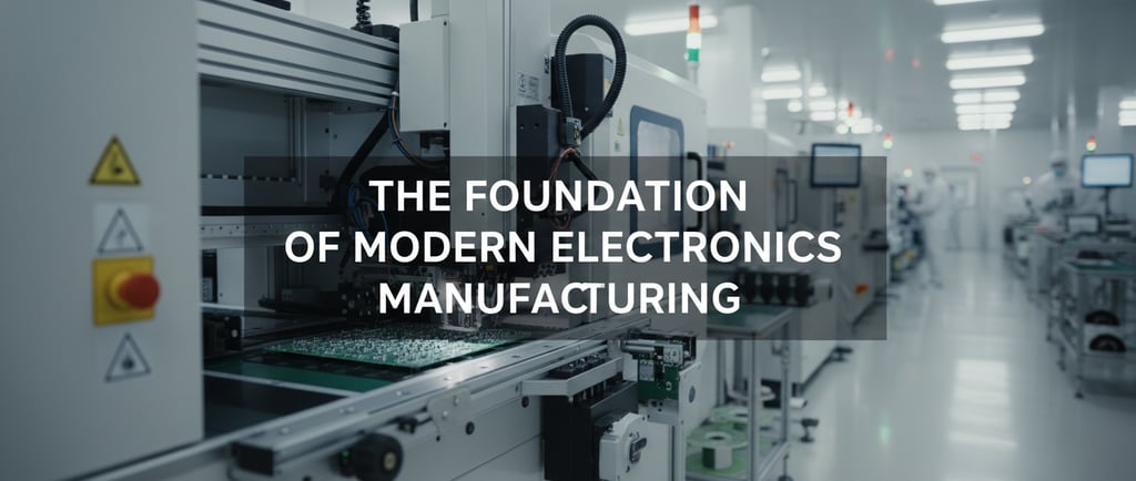
Mastering SMT PCBs: The Foundation of Modern Electronics Manufacturing
Years went by before anything changed - circuit boards built using old-school Through-Hole Tech, parts pushed through drilled openings, fixed down with solder on the backside. Sturdy? Sure. But tight spaces gave it trouble, machines struggled to keep up.
Flying in from the world of compact design - Surface Mount Technology takes center stage. Instead of threading leads through holes, parts called Surface Mount Devices stick right onto the board's face. A quiet change, yet it reshaped how gadgets come together, making room for tighter layouts, faster production, lighter gear, smaller footprints, improved performance where space matters
Tiny parts take up less space. Because of that, more can fit onto a single circuit board. Think about phones or fitness trackers - those slim gadgets need tiny pieces to work. Medical devices implanted in the body? Same story. Size matters when there’s almost no room at all.
Faster operation comes from tighter layouts, where signals travel shorter paths. Less interference appears because unwanted electrical side effects shrink. Signals stay cleaner, opening the door to speed gains. High frequency handling improves when design clutter fades.
Faster builds? Machines handle SMT tasks without pause, repeating moves exactly each time. Precision stays high when robots place parts, never tiring through long runs.
Fine lines of solder carry signals through most modern gadgets you see now. What makes phones thin, computers quick? Surface mounting sticks tiny parts right onto boards.
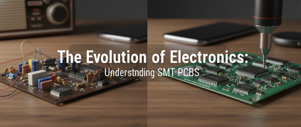
The Evolution of Electronics: Understanding SMT PCBs
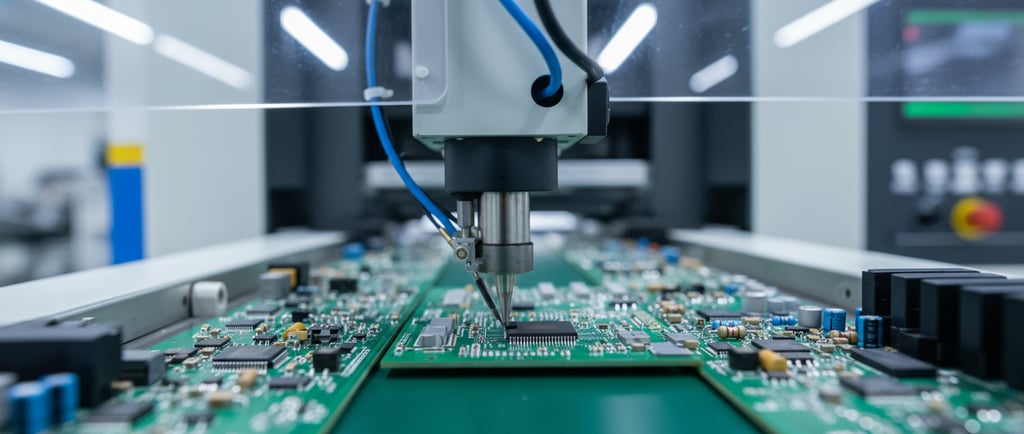
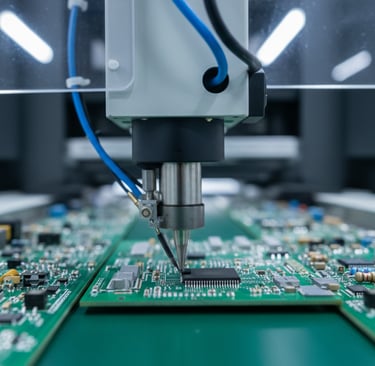
Starting off, putting together a top-notch SMT circuit board takes careful steps done just right. Machines must work sharply, materials need mixing smartly, while people handling them ought to know their craft well. Step by step, here is how it usually goes: one task follows another, each depending on the last
Paste goes on the board before anything else - using a stencil printer spreads it just right across certain spots. That sticky mix? Tiny metal balls swimming in cleaning gel, ready to hold parts down later. Only some areas get coated; the thin sheet guides exactly where. Miss the mark here, one way or another, problems follow fast. Precision matters more than most realize at this stage.
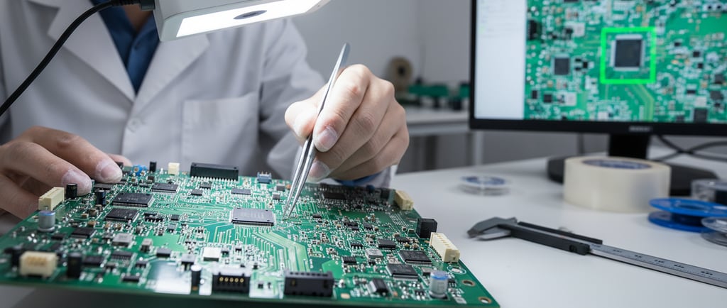
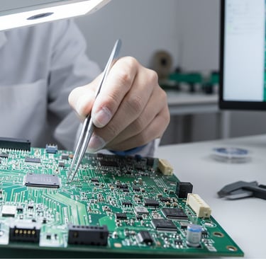
Starting off, tiny parts get set exactly where they need to go after paste goes on. Machines built for speed grab each piece using suction or gentle clamps - pulling them from strips or containers. Accuracy matters here, since every bit lands just right by design. Some units fix small errors themselves thanks to camera-based eyes watching closely. Placement happens fast, sometimes handling twenty thousand bits in one hour alone. Location precision improves because adjustments happen mid-move without stopping.
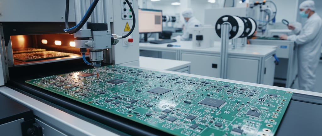
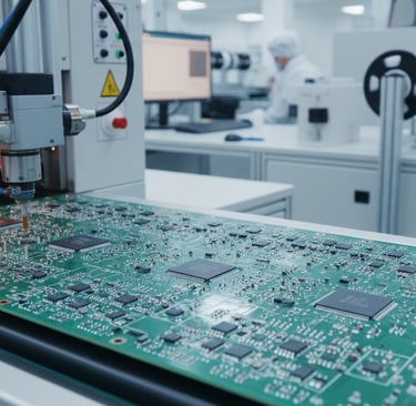
Once parts sit in place, the circuit board moves into a special oven. Inside, different heat stages slowly warm it up so the sticky solder turns liquid. As that happens, connections form between metal pins and surface spots on the board. Heat shifts carefully across sections to avoid harming delicate pieces. When melting finishes, cooling begins right away. Joints harden during this phase, locking everything together securely. Too much warmth too fast might ruin parts or weaken links. Temperature control matters most at every step along the way.
A close look after reflow matters most. What follows reveals how well things held up through heat.
Cameras move fast, checking each board for problems like parts that are gone or placed wrong. Sometimes they catch blobs of solder where they should not be, or spots with too little. What you see is a machine looking closely, spotting what humans might miss. Mistakes show up clearly under those bright lights. Each pass takes just seconds, yet finds issues early. Wrong orientation? It sees that. Missing bits? Noticed right away. The system works without stopping, frame after frame.
Hidden connections on parts such as BGAs or QFNs need special checks. Instead of eyes, machines that see through materials step in. These systems spot tiny gaps where solder should fill. Sometimes wires touch when they should not - this method finds those cases too. Quality control relies on it because flaws stay out of sight otherwise. What looks solid might hide empty spots deep inside. So viewing beneath the surface becomes necessary.
Fresh off assembly, each board faces electrical checks that confirm performance lines up with engineering plans - either through In-Circuit Testing or Functional Testing. One probes individual components while the other mimics real-world operation to see if everything works as intended.
Working alongside trusted builders such as Ominipcba means key tasks get done using modern tools and tight oversight. Their upgraded production setups run smoothly for fast deliveries and large batches of surface mount circuit boards. Every phase, whether laying down solder paste or checking finished units, shows a clear focus on accuracy. Because attention stays sharp from start to finish, results stay consistent.
The SMT Assembly Process: Precision at Every Step
Though SMT brings clear benefits, its distinct hurdles are ones firms such as Ominipcba have learned to move through. Yet not every path stays smooth when speed meets precision.
Key Advantages:
Fewer parts packed into tinier spaces makes gadgets shrink while doing more. Size drops, yet power climbs because components crowd closer than before. Tiny builds come alive when circuits fit tight without losing strength.
Faster signals move through leads that are cut short - this trims both inductance and capacitance. High-frequency operation gains a quiet edge when distances shrink between connections.
What happens when machines take most of the work? Labor expenses drop fast during SMT assembly. Output climbs without needing more people on site. This setup favors large-scale manufacturing simply because it saves money over time. Speed builds up naturally through consistent operation.
Fewer wobbles, less shaking apart - tiny parts stick close to the board, holding firm when bumped. Mounting them flat fights jolts better than older styles ever did.
On two sides they fit parts, using every bit of room. Flipping it over opens more spots for pieces. Space gets packed full when both faces carry bits. Every corner works hard this way. Back and front hold things neatly. Parts sit where needed without waste.
Overcoming the Challenges:
Fixing tiny surface-mount devices isn’t simple. Their cramped layout makes access tough. Precision tools become essential in these tight spots. Expert hands handle what machines start. Mistakes here risk nearby components. Each move needs careful planning. Skill shapes success more than speed ever could.
Starting too hot might fry delicate parts during reflow soldering. A wavy heat path through the board risks weak connections. Sudden drops near the end often leave joints brittle. Each stage needs careful timing - too slow cooks the circuitry. Too fast misses proper melting. Uneven warmth creates hidden flaws that show up later. Machines must adapt on the fly to keep things stable.
Fragile by design - some surface-mount devices react badly to static electricity or humidity. That means care is non-negotiable during storage or movement. Rules must be followed without exception. Mistakes lead to damage you can’t see. Protection starts before unpacking even begins.
Because placing solder paste and parts demands exactness, costly machines built for precision become necessary. Machines that handle tiny components must work without error, so their build quality drives up cost. When even a fraction of a millimeter matters, only advanced equipment can deliver results. Precision tools dominate here since mistakes are not an option. Their expense comes from the need to perform perfectly every single time.
A single mistake in SMT layout can cause big problems later. Think ahead about how parts will be made when setting up the design. Skipping this step often leads to faults that slow everything down. Making space between components helps machines place them correctly. Wrong choices early might mean rework after production begins. Small adjustments now reduce errors during assembly. Layout decisions directly affect whether boards come out right the first time.
Tackling problems straight away, Ominipcba pours resources into advanced SMT machines. Before production kicks in, design flaws get caught early thanks to thorough DFM checks. Clean rooms stay stable - humidity watched closely, static risks blocked by ESD safeguards. Skilled engineers plus sharp-eyed technicians handle each build with care. Reliability grows when every detail is shaped ahead of time. Complex layouts? They move through the line without skipping a beat. Strong results come not from luck, but steady groundwork done right.
Advantages and Challenges of SMT PCB Assembly
A tiny flaw during SMT PCB assembly might ruin a whole device, triggering expensive fixes, breakdowns after delivery, or harm to a company's standing. That’s the reason having a full QA system isn’t just helpful - it’s essential.
Fine details matter when checking SMT work - eyes alone aren’t enough. Through careful steps, one step follows another quietly but surely
A fresh look at how parts come together begins before anything is built. Spotting hiccups early keeps production smooth later on. Problems show up quietly in sketches, not on factory floors. Tweaking blueprints ahead of time saves effort down the road. Ideas shift slightly here so reality fits better there. Small changes now prevent big delays soon after.
Temperature checks inside ovens help track how parts stick together. What matters most? How much goop gets spread each time. Machines place pieces - watching if they land right is key. Mistakes show fast when settings drift off target.
Tiny flaws escape people but machines catch them. Cameras scan surfaces where vision fails. X rays reveal what light hides. Systems flag irregularities without pause. Precision drives every check. Mistakes vanish under electronic gaze. Repetition never dulls their focus. Each circuit gets full attention. Flaws too small to name are found anyway.
Testing electrical performance means using tools like In-Circuit Test alongside Functional Circuit checks. These methods confirm the built board works right. Each check runs separately yet complements the other. One spots tiny faults. The other verifies real-world operation. Together they cover more ground than either alone.
Every part gets logged. Step by step, each move is written down. Details stick around for review. Each phase leaves a paper trail. Nothing slips through unseen.
From the moment components arrive, Omnipcba watches each step of the SMT PCB build with tight oversight. Because they follow ISO-approved methods and keep refining their work, every circuit board they send out runs dependably under tough demands. It is this relentless focus on excellence that turns a basic production line into something closer to a trusted collaborator.
Why Quality Assurance is Non-Negotiable in SMT PCB Assembly
Fine wires inside tiny boards make today's gadgets work quicker, thinner, lighter. Though they bring strong results, handling them well means deep knowledge, sharp tools, staying focused on precision every step.
When engineers or product managers grasp how SMT PCB assembly works, better choices follow - choices shaping speed, function, quality. A well-matched manufacturer unlocks what the technology can truly deliver.
Here’s something to think about: when exactness matters, speed counts, or handling everything in one go is key, going straight to Ominipcba might just clear up confusion. Their team knows the ins and outs of PCBA work, having seen nearly every twist that can pop up. Quality isn’t guessed at - it shows up consistently, built into each step. Instead of juggling multiple suppliers, a single source could save time, reduce errors, then free up energy for what comes next. Products tend to run smoother, last longer, behave better once tested. For those tired of hiccups halfway through manufacturing, getting in touch may quietly shift how things move forward.
Conclusion & Next Steps
Frequently asked questions
Q: What is an SMT PCB?
A: An SMT PCB (Surface Mount Technology Printed Circuit Board) is an electronic circuit board populated with components (SMDs) that are soldered directly onto the surface of the board, rather than having leads inserted through holes.
Q: What are the main advantages of SMT PCB assembly?
A: The main advantages include enabling miniaturization of electronic devices, higher component density, improved electrical performance, enhanced automation in manufacturing, and increased reliability.
Q: How does SMT differ from Through-Hole Technology (THT)?
A: SMT components are mounted directly on the PCB surface, while THT components have leads that pass through holes in the board. SMT allows for smaller components and greater automation, while THT is often used for larger, higher-power components.
Q: What are the key stages in the SMT assembly process?
A: The key stages typically include solder paste application, automated component placement (pick-and-place), reflow soldering, and comprehensive inspection (AOI, AXI).
Contacts
Email: sales@ominipcba.com
Mobile: +86-185-7640-5228
Copyright © 2007-2026. Omini Electronics Limited. All rights reserved.
Head Office: +86-755-2357-1819
Services
Your China turnkey partner for electronics manufacturing. We bridge design to delivery by leveraging the Shenzhen electronics ecosystem for precision engineering and streamlined PCBA supply chain logistics.
Ready to Build?
Get a comprehensive quote within 24 hours.
