Phone: +86-755-2357-1819 Mobile: +86-185-7640-5228 Email: sales@ominipcba.com whatsapp: +8618576405228

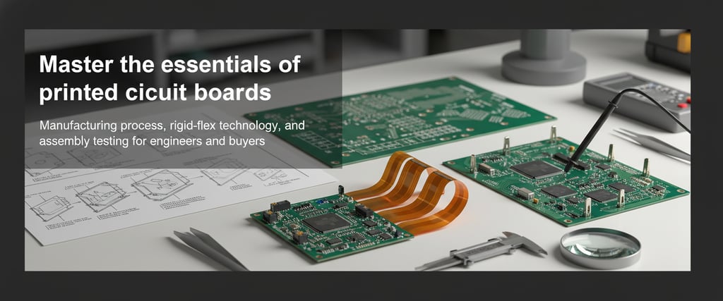
The Hardware Pro’s Guide to PCB Anatomy: From Stack-Up to Assembly
Master the essentials of printed circuit boards. We break down the PCB manufacturing process, rigid-flex technology, and assembly testing for engineers and buyers
PCB TECHNOLOGY
Amanda
2/5/20253 min read
From the smartphone in your pocket to the industrial MCUs powering automation, printed circuit boards (PCBs) are the silent heartbeat of modern technology. But for hardware engineers and procurement professionals, a PCB is far more than a simple substrate—it is a sophisticated integration of material science and electrical engineering that defines a product’s reliability and performance.
Whether you are optimizing a Bill of Materials (BOM) or routing high-speed differential pairs, understanding the intricacies of the manufacturing process is essential. Here is a professional breakdown of the critical elements that define a high-quality board.
The Architecture: Optimizing the PCB Stack-Up
In high-performance electronics, the PCB stack-up is the blueprint for signal integrity. This strategic arrangement of conductive and insulating layers dictates everything from impedance control to thermal dissipation.
Substrate (Core): Typically FR4 (Flame Retardant 4), providing the necessary mechanical rigidity and dielectric constants.
Copper Foil: The conductive pathways. Measured in ounces (e.g., 1 oz, 2 oz), the copper weight determines the board's current-carrying capacity.
Prepreg: The "bonding" layer that fuses multiple layers together during the lamination process.
Solder Mask: A protective polymer coating—available in green, blue, black, or custom matte finishes—that prevents copper oxidation and eliminates solder bridging.
From a PCB fabrication standpoint, the stack-up is the most vital file sent to the fab house. It is the foundation for managing high-speed signal transitions and power-hungry circuits.
Rigid, Flex, and Rigid-Flex: Selecting the Right Substrate
While standard FR4 boards satisfy most applications, complex industrial designs and compact form factors often require specialized substrates:
Rigid PCBs: The industry workhorse—durable, cost-effective, and ideal for standard electronics.
Flexible PCBs: Built on polyimide bases, these allow for 3D routing and are essential for wearables and dynamic applications like print heads.
Rigid-Flex PCBs: A hybrid solution where rigid sections are interconnected by integrated flexible ribbons. While the initial cost is higher, rigid-flex reduces the total BOM cost and assembly time by eliminating bulky connectors and wire harnesses while significantly improving reliability in high-vibration environments.
The Assembly Phase: SMT vs. Through-Hole (PTH)
After fabrication, the bare board enters PCBA assembly. Choosing the right mounting technology is critical for balancing manufacturing throughput with physical durability.
Surface Mount Technology (SMT)
The gold standard for modern electronics. Components are placed directly onto surface pads via high-speed pick-and-place machines and soldered in a reflow oven. SMT enables high component density and double-sided population, maximizing PCB real estate.
Through-Hole Technology (PTH)
Leads are inserted through drilled holes and secured via wave or selective soldering.
The Technical Verdict:
Specify SMT for 95% of components to minimize footprint and manufacturing cycle times.
Specify Through-Hole for high-stress components, such as heavy-duty connectors, power transformers, or large electrolytic capacitors, where mechanical bond strength is paramount.
Quality Assurance: Inspection and Testing Protocols
Reliability is non-negotiable. At OminiPCBA, we utilize rigorous verification stages to ensure every board meets IPC standards:
ICT (In-Circuit Test): A "bed of nails" fixture provides high-speed electrical verification for mass production.
Flying Probe Testing: A fixtureless robotic probe system, ideal for low-to-medium volume prototypes where speed and flexibility are required.
AOI (Automated Optical Inspection): High-resolution cameras detect assembly defects such as "tombstoning," polarization errors, or insufficient solder joints.
Pro Tip: Incorporating Design for Testability (DFT) during the layout phase is a critical best practice. Including dedicated test points allows for automated ICT, preventing the high labor costs associated with manual troubleshooting.
Partner with OminiPCBA for Seamless Hardware Execution
Navigating the complexities of layer stack-ups, global component sourcing, and advanced assembly can be a bottleneck for any engineering team.
At OminiPCBA, we act as a strategic partner. From comprehensive DFM (Design for Manufacturing) reviews to managing the full turnkey supply chain for complex PCBA builds, we ensure your hardware reaches the market with zero defects.
Let us handle the complexities of fabrication and assembly so you can stay focused on innovation.
Related Articles
Contacts
Email: sales@ominipcba.com
Mobile: +86-185-7640-5228
Copyright © 2007-2026. Omini Electronics Limited. All rights reserved.
Head Office: +86-755-2357-1819
Services
Your China turnkey partner for electronics manufacturing. We bridge design to delivery by leveraging the Shenzhen electronics ecosystem for precision engineering and streamlined PCBA supply chain logistics.
Ready to Build?
Get a comprehensive quote within 24 hours.
