Phone: +86-755-2357-1819 Mobile: +86-185-7640-5228 Email: sales@ominipcba.com whatsapp: +8618576405228


Ultimate Guide to PCB Copper Thickness
Explore the essential aspects of PCB copper thickness in our comprehensive guide. Learn about its role in PCB stackup, impact on electrical and thermal performance, and how to choose the right copper
PCB MANUFACTURING
Amanda
12/1/20242 min read
2. Thermal Management: Copper helps dissipate heat generated by electronic components.
3. Corrosion Resistance: Copper’s resistance to corrosion ensures longevity in PCB designs.
4. High-Performance Suitability: Copper is ideal for high-speed, high-frequency PCB designs.
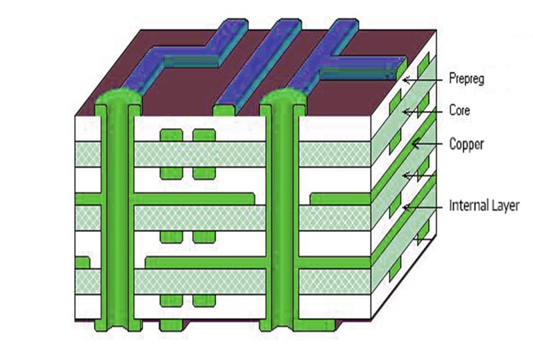
PCB Stackup: Understanding Layers and Copper’s Role
The PCB stackup defines the total board thickness and consists of several layers that are glued together. Here’s a breakdown of the stackup layers:
1. Copper Foil: Responsible for current flow through traces and circuits (Cu).
2. Prepreg: Bonds the layers of the PCB stackup together.
3. Core/Substrate: Acts as the base for the circuit components (typically FR4 or other materials).
Copper plays a central role in PCB functionality by enabling current flow through the traces etched onto the copper foil, connecting all the active and passive components. Omini ensures that the copper layer is designed and optimized to meet the specific needs of your PCB applications.
What is PCB Copper Thickness?
PCB copper thickness refers to the amount of copper deposited per square foot of the PCB area. Copper thickness impacts the board’s electrical, mechanical, and thermal performance. In multi-layer PCBs, copper layers are stacked in both the inner and outer layers to support current flow and signal integrity.
Standard PCB Copper Thickness
The most common standard copper thickness for PCBs is 1 oz per square foot. This translates to a thickness of 35 micrometers (0.0335mm or 1.4 mils). However, designers can choose varying copper weights based on performance requirements. Copper options include 0.5 oz, 1.5 oz, 2 oz, and more, with each providing different performance characteristics.
Advantages of 1oz Copper Weight
1. Balanced Conductivity and Thermal Management: Ideal for most PCB applications.
2. Cost-Effective: Affordable for mass production and readily available.
3. Durable: Provides strength and durability under physical stress.
1oz copper is widely used due to its balance of cost, performance, and reliability in meeting design criteria.
Key Considerations in Selecting Copper Thickness
Selecting the appropriate copper thickness is critical to meeting specific design requirements. Here are several factors to consider:
1. Current Rating
High current applications may require thicker copper to handle increased thermal dissipation and prevent voltage drops that can lead to board failure.
2. Mechanical Toughness
For PCB applications subject to bending or stress, thinner copper is preferable to maintain flexibility and prevent damage.
3. Number of PCB Layers
Multi-layer boards require higher copper thickness (greater than 1 oz) to support power and signal integrity.
4. Clearance and Creepage
Higher copper thickness affects trace spacing, which must be considered to avoid short circuits and ensure safe operation in high-voltage designs.
Conclusion
Copper thickness directly influences the performance of your PCB. By carefully selecting the appropriate copper weight, Omini ensures that your PCB will meet all electrical, thermal, and mechanical performance standards. Clear communication with your manufacturer and accurate stack-up data are essential for maintaining the design lifecycle and avoiding potential issues during production.
At Omini, we understand the importance of precise copper selection and are committed to providing you with high-quality, reliable PCBs tailored to your specific needs.
Printed circuit boards (PCBs) transform ideas into functional electronic devices, and this process heavily relies on one essential component: copper. The copper layer in a PCB is integral to its electrical, mechanical, and thermal performance. At Omini, we understand the critical role copper plays in PCB design and manufacturing. This guide provides a comprehensive overview of copper thickness in PCB stackup, helping designers optimize their designs.
The Role of Copper in PCB Stackup
Copper is a versatile and widely used metal, essential for various applications, including PCBs. The key functions of copper in PCBs include:
1. Electrical Conductivity: Copper is the best conductor of electricity, allowing the current to flow through the PCB.
Contacts
Email: sales@ominipcba.com
Mobile: +86-185-7640-5228
Copyright © 2007-2025. Omini Electronics Limited. All rights reserved.
Head Office: +86-755-2357-1819
Products & Services


Office Address: No. 605, Tongxin Technology Building, Bao’an Avenue, Bao’an District, Shenzhen, Guangdong, China.
Factory Address: Buildings 5 and 12, Lisheng Industrial Zone, Tangwei Community, Fuhai Street, Bao'an District, Shenzhen, China.
Omini Electronics Limited is an expert in trusted PCB Fabricaton and PCB Assembly in China since 2007. We have served over 1000 global customers with high-quality, low to medium-volume production. Certified by UL (E532498), ISO9001:2015, and ISO13485:2016, we offer expert electronics manufacturing services, including PCB manufacturing, assembly, and contract manufacturing, ensuring top-tier quality and precision in every project.