Phone: +86-755-2357-1819 Mobile: +86-185-7640-5228 Email: sales@ominipcba.com whatsapp: +8618576405228

AI Server Interconnects: Engineering the 1kW Thermal Frontier
AI hardware demands extreme fabrication precision. We analyze embedded cooling, 40-layer stackups, and the SMT challenges of high-density AI server PCBs.
PCB TECHNOLOGYPCB MANUFACTURINGPCB ASSEMBLY
OminiPCBA
1/14/20267 min read
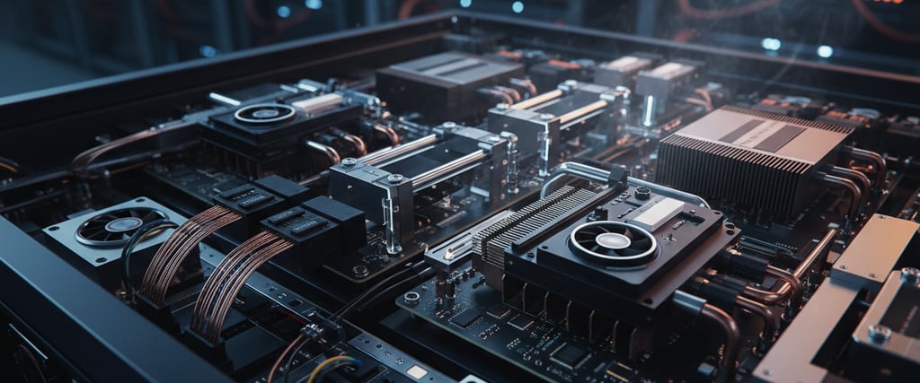
Heat and power shape how AI systems are built, more than software ever could. When machines learning huge models grow past a trillion pieces of data, what holds them together changes form. Circuit boards stop being just platforms holding parts. They become active systems handling massive electric loads while moving oceans of information at once. Building these isn’t routine work - it pushes factory skills to their breaking point. Machines bending metal and copper must perform near impossible precision tasks. Each piece connects under extreme conditions where even tiny flaws cause failure. These aren't old-style electronics anymore - they behave like engines made of signals and heat. Factories producing them operate at the edge of what modern industry can achieve.
The Thermodynamic Crisis Rethinking How Heat Escapes
Heat limits how we build AI servers. Not just power - these new chips push so much heat they break normal circuit boards. Take today’s top GPUs and TPUs - they often run between 700W and 1000W each when packed into HPC setups. Eight of them on one baseboard? That kind of energy doesn’t stay contained. Standard FR-4, the usual board material, can’t handle it - it peels apart under stress like wet paper left too long in sun.
Tiny metal holes meant to move heat fall short when packed too tight. Yet engineers found a better path. Instead of relying on those, they now tuck thick copper disks right inside the board. These coins - called T, I, or U types - sit flush within the layers. Heat escapes faster this way. Performance keeps up without slowing down. Behind the scenes, the design runs cooler by cutting resistance at the source.
Here’s where things get tricky - fitting the copper coin isn’t just slotting it in place. Instead, it needs to be locked inside a milled pocket in the board prior to layer stacking. Pressure seals everything together only after positioning. What complicates this: materials react differently when heated. As temperature rises, copper stretches slowly - about 17 parts per million per degree. But the insulating resin nearby? It swells faster, each type moving at its own pace. When resin shrinks too much or spreads unevenly while making the board, the connection between the coin and the circuit panel can crack under intense heat during assembly. Manufacturing records from sources such as Ominipcba show that staying extremely close to design specs - usually within 0.05mm for how flat the coin sits - is key because even small air pockets block heat flow.
Heavy Copper and Power Delivery Networks
What makes things hot isn’t just the chip. Moving 1000 amps at 0.8 volts to a graphics processor demands serious power flow. Because resistance eats energy as heat, special circuit boards pack thick copper inside - anywhere from 3 oz up to 6 oz, that is 105μm through 210μm. So much current means materials must handle the load without burning off efficiency.
Starting deep inside the metal, carving through two hundred microns demands precision chemistry. Vertical progress matters, yet sideways erosion risks ruining thin pathways nearby. A sharp tilt along the edge changes how electricity moves across the circuit. That shift can disturb timing cues essential for waking up the graphics processor correctly.
Vertical Scaling With Over Thirty Layers
Even though strength sets how thick things get, speed needs decide how many levels are packed in. Machines running smart tasks talk fast using rules such as PCIe Gen 6 and 112G PAM4 so they respond almost instantly. For signals not to mess each other up, every one hides behind grounded shields built like a stripline setup.
A single 40-layer board might reach close to 5 millimeters in height. Because of that thickness, making a tiny hole just 0.2 millimeters wide becomes tricky. The deeper the board, so goes the challenge - drilling through creates stretched proportions called aspect ratios. Most high-end AI boards now pack anywhere from 24 to 44 levels stacked tight. When you pierce such density at small scales, the math shifts sharply - ratios often climb past 25 to one.
Deep inside tiny holes, getting copper to stick evenly needs a special mix. Instead of spreading smoothly, regular solutions pile up near the opening, leaving gaps deeper down - like a bone with swollen ends. Heat changes can break weak spots where metal runs thin. To fix this, some makers use quick bursts of current that flip direction, building steady walls of copper all the way through. Every bit must measure exactly 25 micrometers thick; anything less won’t hold up when things get tough.
Material Science Meets Low Loss Demands
When signals go above 28 GHz, the insulating layer in circuit boards starts weakening them. Instead of moving forward, some energy gets soaked up by regular FR-4 resin. That absorbed power turns into warmth, which wastes performance. Because of this behavior, making servers powered by artificial intelligence means choosing advanced alternatives. Materials like Megtron 7 or 8 from Panasonic come into play - also Isola's Tachyon series joins that group along with certain Rogers blends built for speed.
Not so long ago, signals stayed clean across distances thanks to materials with less than 0.002 dissipation factor. Still, their structure behaves little like regular epoxy resins. Being on the fragile side, they tend to snap easier when bent. Because of weak layer bonding, peeling forces don’t last very long. Drilling into them gets tricky - too fast and tiny cracks spider through the fiberglass. Much of the time, dampness gets into these high-tech layers easily. Because of that, keeping air wetness low inside storage areas matters a lot. Before sealing them together, long oven drying steps must happen. That way, steam does not grow when heat is applied later on.
The Signal Integrity Challenge With Back Drilling
Starting deep within a 30-layer board, a signal could journey from the surface down to Layer 8. Beyond that point, what's left of the metal-coated hole stretches all the way to Layer 30 without doing any real work. When AI systems push data at blazing speeds, this idle leftover behaves like a tiny echo chamber. It bounces energy back where it came from, muddying the original flow - loss creeps in. That ghost reflection? Pure trouble for clean signals.
Manufacturers handle this by using Controlled Depth Back-Drilling. A drill bit just wider than the via scrapes out extra copper from inactive layers. Tiny margins matter here. Past Layer 8, one slip ruins the working trace below.
One wrong move and everything shifts - accuracy must stay within 150 microns. A bit shy of full depth leaves a remnant capable of disrupting 112G transmission. Go just slightly past target and the connection breaks entirely. Some shops, like Omnipcba, rely on smart drilling tools that feel their way down until hitting buried copper, then stop dead. That instant pause keeps pathways clean while holding the board together.
Smt Assembly For Big Size Boards
Moving from making blank circuit boards to putting parts on them brings fresh physical problems. Not small by any measure, AI server baseboards frequently go beyond the usual 18x24 inch sheet limit. Their broad shape means they can bend under their own weight when heated in the soldering process.
Starting at one end, the circuit board moves into a heating chamber where heat climbs close to 245°C. Copper layers sandwiched between glass fibers and resin stretch unevenly when hot. A tiny bend - just one percent - and those large chip packages used for processors can’t form proper joints. Often, what happens next looks like this: the round blob of metal flattens out but misses merging with its matching spot of wet paste below. That gap comes from warped surfaces. It acts fine during checks right after assembly. Stress changes everything later.
Fixturing and Thermal Profiling
Floating through heat without bending hinges on how well the load rides. A custom cradle built from stuff such as Durostone holds firm beneath the middle. Balance stays true because structure answers distortion.
Heat moves slow through thick copper stacks. When a circuit board packs twenty layers plus dense metal inserts it acts like a heat sponge. Slow warming keeps temperatures even inside. Without enough time in the pre-melt phase cold spots linger below. Melting solder too fast risks weak joints. Long exposure at moderate levels pulls hidden zones up to speed. Balance matters more when mass resists change.
Heat moves through a dense fluid during vapor phase soldering. This method shows up in top-tier electronics manufacturing when precision matters most. Instead of relying on hot air, it immerses boards in heated vapor. Uniformity improves because the liquid spreads warmth evenly. Big circuit assemblies see less temperature variation from one spot to another. Delta-T drops without needing extra adjustments.
HDI Microvia Reliability
Getting thousands of signals off a big BGA chip demands tight, layered wiring - regular designs just won’t work. Layer stacks like 3+N+3 or 4+N+4 show up often on AI hardware, built with several levels of tiny laser-made vias.
Stacked microvias - those lined up straight through layers - get close attention because they tend to weaken over time. Heat changes stress the connection where one via meets another, making that spot likely to crack. Instead of lining them up, engineers often shift each via slightly on the next level, which holds up better. If alignment can’t be avoided, the holes are packed tight with plated copper, forming a continuous rod-like structure that boosts both strength and electrical flow.
Inspection Limits and How They Are Addressed
Hidden beneath GPUs and copper coins, vital solder joints on AI server boards escape traditional AOI checks. Seeing through layers takes more than light alone. With X-rays, inspectors bypass surface limits entirely. Instead of relying on visibility, they peer inside using 3D imaging. This method reveals what optical scans cannot catch. Engineers then assess solder gaps by measuring voids within each connection point. Standard practice now leans heavily on AXI for such deep analysis.
Most times, air pockets beneath the heating element stay under 15-20% when building AI systems. Too many gaps lead to uneven warmth, slowing down cooling. Test samples often go through stress checks that mimic long-term temperature swings - this shows whether thick copper layers inside holes can survive constant shifts without breaking over time.
The EMS Paradigm Shift
Now making AI server circuit boards doesn’t follow a straight path like print, then etch, next build. Instead, it pulls together experts - material researchers work alongside structural designers while surface mount tech leads keep pace. Choices come fast - one pick boosts electricity flow yet makes chemical shaping harder. More layers help signals stay clean though drill precision suffers. Built-in cooling fixes heat problems but adds pressure during pressing stages.
In the EMS world, generative AI isn’t merely a chance to grow - it pushes companies to sharpen their tech depth. Not every maker keeps pace; only those fine-tuned for precision thrive where physics meets circuit demands. When blueprints stretch into dense stacks of copper and mixed layers, success hides in flawless output. High-volume results on intricate 40-layer boards separate tomorrow's key players from the rest. Complexity grows, yet consistency wins.
Related Articles
Contacts
Email: sales@ominipcba.com
Mobile: +86-185-7640-5228
Copyright © 2007-2026. Omini Electronics Limited. All rights reserved.
Head Office: +86-755-2357-1819
Services
Your China turnkey partner for electronics manufacturing. We bridge design to delivery by leveraging the Shenzhen electronics ecosystem for precision engineering and streamlined PCBA supply chain logistics.
Ready to Build?
Get a comprehensive quote within 24 hours.
