Phone: +86-755-2357-1819 Mobile: +86-185-7640-5228 Email: sales@ominipcba.com whatsapp: +8618576405228

AR/VR PCB Engineering: The Weight vs. Performance Paradox
Solving the density crisis in AR/VR hardware. A deep dive into mSAP, rigid-flex architectures, and thermal strategies for next-gen wearables.
PCB TECHNOLOGYPCB MANUFACTURINGPCB ASSEMBLY
OminiPCBA
1/18/20266 min read
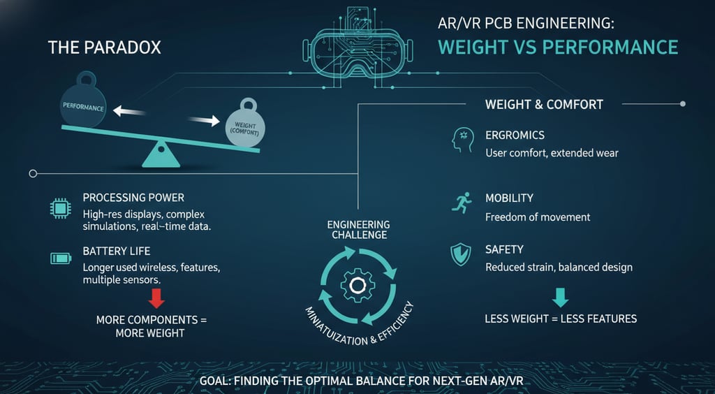
Chasing the dream of fitting a computer's strength into something as light as reading glasses drives XR tech forward. On the edge of what factories can build, AR and VR wearables push limits like nothing else. While phones sit comfortably in hand, these gadgets balance on your face - making each ounce feel heavier. Space vanishes fast when you're designing for the space between your eyes. Tiny shifts in size or heft aren’t just details - they decide whether it works at all.
Now space fights heat in every tiny circuit board made. Boards lie flat less often, instead bending into shapes that hug cameras and power packs tightly. Thinking beyond screens pushes old layered designs aside, replacing them with compact base-style builds. Fitting parts close means dealing with warmth differently, shielding shifts subtly, cooling adapts quietly inside tight shells.
The Density Crisis Beyond High Definition Imaging
Usually, regular gadgets work fine with an HDI board built as 2+N+2 - just two layered sides around a center piece. Still, AR glasses pack too much: GPU, motion sensors, fast wireless chips, screen controllers - the kind of crowd that overwhelms standard etch-routing tricks.
Folks are jumping fast on Any-Layer HDI - also known as ELIC. Without a middle core at all, it lets vias pile up from top to very bottom. That open path means parts fit anywhere, front or back, since no space gets lost to old-style holes.
Now things get tricky as line widths and gaps shrink below 30 microns. Because regular etching struggles here - copper lines end up fatter at the bottom, like a sloped trapeze. So better factories shift toward something called mSAP instead. Rather than carve out copper, they grow it precisely on a slim starter coat. Photomasks define the shape, then metal fills in only where needed. This method creates straight-walled traces, more box-like than wedge-shaped. Clean edges mean consistent electrical paths even when signals pack tight together. Better geometry helps manage resistance and reduces interference inside compact audio gear.
Rigid Flex The Foldable Circuit
Curved shapes change how things fit together. Because the skull wraps around, gear inside has to follow its form instead of fighting it. A single stiff board would leave gaps where nothing works right. Parts need to link across distances without losing contact. Flexible circuits bend into place while keeping strength where needed. These connections run like pathways under the skin of the device. Sensors up front talk through them to power packs behind. Electronics adapt to people rather than the other way around.
Building these circuit boards means understanding how materials bend under pressure. Where stiff fiberglass connects to bendy plastic - that spot matters most. Think of a virtual reality headset band moving back and forth all day. That joint gets twisted over time, again and again. To handle it, makers add slim protective layers shaped like curves, along with rounded glue beads. These help spread out the strain before cracks start.
Moisture hiding in polyimide can blast apart boards when heated, so baking it first makes sense. Ominipcba tracks standards where this step shows up again and again. Steam forms fast if damp film meets solder heat, wrecking delicate layers. Vacuum sealing after drying keeps everything locked tight. Tough multilayer builds survive only when each phase respects the physics at play.
Heat Control and the Human Element
Heat puts hard limits on how well AR and VR devices run. While a desktop graphics chip might hit 90°C with no trouble, the computer inside a headset can’t go nearly that high. Human skin sets the boundary - devices must stay around 40°C to 45°C at the surface. Go beyond that, irritation kicks in, sweat appears, then fog rolls across the lenses.
Heat moves fast when metal helps. A coin of copper tucked inside the board pulls warmth down from hot chips. That heat travels through the layers until it reaches the far side. There, a housing made of magnesium takes over. Or maybe a flat chamber filled with vapor does the job instead. The circuit board is more than wiring - it spreads thermal energy too.
Still, moving heat around does little unless guided properly. Thin layers of graphite, able to channel warmth sideways fast - nearly 1500 W/mK - are pressed flat against the circuit board. Getting those pieces exactly where they belong becomes the real test for the assembly team. Misplace one so it links two connection points, and suddenly there's an unintended path for electricity. A break in the thermal path happens when alignment fails. For large-scale manufacturing, optical-verified automation stands as the sole practical option.
Signal Quality and Electromagnetic Protection
Faster than a blink, virtual reality stumbles if delays creep past twenty thousandths of a second. Signals sprinting through MIPI or PCIe pathways must weave right beside radio-sensing zones like those for 5G and wireless links. Squeeze it all into tight quarters, interference pops up everywhere like sparks in a storm.
Heavy metal enclosures take up too much space in augmented reality eyewear. Instead, engineers use segmented barriers alongside vapor-deposited thin-film shields. These methods save room while maintaining protection levels needed for sensitive circuits.
Fences dug into the board’s base layer form pockets. These gaps get filled with metal goo, building tiny shields right inside the material. Walls rise where copper stops, blocking stray signals before they spread.
A fine coat of conductive stuff covers the whole module after SMT work finishes. This happens through spraying or sputtering, just enough to shield without adding bulk.
Nowhere else does space saving come at such a cost to repairability. When coating seals the module, swapping out a faulty chip becomes unworkable. That reality sharpens the focus entirely on getting it right the first time. With SMT assembly, success hinges on near-flawless execution from the start.
The Assembly Challenge 008004 and Underfill
When tiny parts get as small as a speck - like the 008004 size at 0.25mm by 0.125mm - the way solder paste behaves during printing shifts. Because the hole in the stencil becomes extremely narrow, paste sometimes sticks due to surface forces, refusing to drop on the pad.
Some leading full-service PCBA companies now choose Solder Jet Printing to tackle these issues. Instead of using stencils, this method propels tiny blobs of solder paste directly onto landing spots with extreme precision. That sharp alignment matters most on boards with sunken areas, where parts fit into lowered zones to reduce overall thickness.
When devices you hold or wear get bumped, tiny parts inside can shift. To stop that, a special glue goes between the chip and the circuit board. This sticky stuff holds everything tight, especially if the board bends a little when someone moves their head. Without it, the metal connections might break over time. How the liquid spreads matters just as much - it sneaks into gaps on its own but must stay clear of light sensors nearby. Too much spread causes problems nobody wants later.
Mini LED and Micro OLED Optoelectronics Integration
A sharp image in XR gear starts with advanced screens. Because Micro-OLED and Mini-LED grids demand it, the base circuit board must stay perfectly even and steady.
Thousands of tiny LEDs need attaching to the base layer in Mini-LED backlights. Heat builds up across those small lights during operation. That warmth might twist the board if unchecked. A bent circuit panel throws off how evenly light spreads through lenses above. So materials resisting heat distortion become essential - especially ones that barely expand when warm.
Apart from standard methods, tiny chips driving these screens usually attach through wire bonds right onto the board, cutting down on room needed. Bare silicon parts then show up during build, making dust control critical - air quality must match Class 1000 cleanrooms or tighter, way beyond average circuit board lines. Places such as Ominipcba now run mixed setups, blending surface mount tech with processes once saved for chip sealing.
System-in-Package (SiP) Evolution
One tiny package now holds what once took many separate parts. Instead of stacking individual pieces, everything fits inside a single compact unit. This small block contains the brain, storage, power control, and supporting elements. It resembles a big chip, but does far more than before. Designers choose this approach when space is tight. The whole setup gets sealed together during manufacturing. Less room is needed on the circuit board because of it. Each component works as one from the start. Size drops sharply without losing function. What used to spread across inches now fills just millimeters.
Now the EMS role changes completely. Simpler motherboards show up, yet the real challenge hides inside the SiP's base layer instead. That tiny foundation works like a miniature circuit board, sometimes needing lines just 10 to 15 microns wide. Spotting flaws means using X-rays plus live performance checks on bare chips prior to sealing them in plastic, because one flaw dooms the whole costly unit without recovery.
The Making of Invisible Structures
Hardware wins when you forget it exists. Feel matters more than features - comfort hides bulk, cooling beats overheating. Seeing clearly means ignoring the machine on your face. Engineering magic happens where no one looks: deep inside circuit boards. Good design vanishes; only experience stays.
Tiny wires, more layers, tinier parts - that is where building chips and boards now leads. Heat control and clean signals must shape design from day one, not tagged on later. When the Metaverse shifts from idea to actual gear, success hinges on makers skilled at balancing size limits with physical laws. Who wins in the device race depends heavily on those who blend engineering grit with precision build. Machines rise or fall by the hands that mold their bones.
Related Articles
Contacts
Email: sales@ominipcba.com
Mobile: +86-185-7640-5228
Copyright © 2007-2026. Omini Electronics Limited. All rights reserved.
Head Office: +86-755-2357-1819
Services
Your China turnkey partner for electronics manufacturing. We bridge design to delivery by leveraging the Shenzhen electronics ecosystem for precision engineering and streamlined PCBA supply chain logistics.
Ready to Build?
Get a comprehensive quote within 24 hours.
