Phone: +86-755-2357-1819 Mobile: +86-185-7640-5228 Email: sales@ominipcba.com whatsapp: +8618576405228

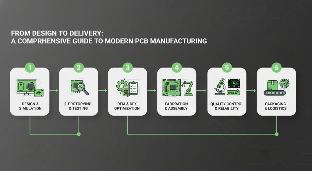
From Design to Delivery: A Comprehensive Guide to Modern PCB Manufacturing
At Omini PCBA, we believe that the most successful hardware products start with a deep understanding of the manufacturing floor. Printed Circuit Boards (PCBs) are far more than just "green boards"; they are the high-precision nervous systems of modern technology. As the industry scales toward a projected $100 billion market by 2030, the gap between a digital design and a functional physical product is bridged by a series of rigorous, machine-driven steps. This guide breaks down exactly how these boards are built, from the first Gerber file to the final electrical test.
PCB TECHNOLOGYPCB MANUFACTURINGPCB ASSEMBLY
OminiPCBA
2/27/20263 min read
The Anatomy of a PCB: The Four Essential Layers
Before diving into the machinery, it is important to understand what makes up the board itself. Every standard PCB is a composite of four distinct materials:
The Substrate: Typically made of FR-4 fiberglass, this provides the "skeleton" of the board. It ensures rigidity and prevents the assembly from snapping under mechanical stress.
The Copper Layer: This is the lifeblood of the circuit. Whether it’s a thin foil or a heavy coating, this conductive layer carries electrical signals between components.
The Solder Mask: This is the board’s "skin." It protects the copper traces from oxidation and prevents accidental shorts during the soldering process.
The Silkscreen: Also known as the legend, this layer adds the human-readable text—part numbers, logos, and reference designators—that makes assembly and troubleshooting possible.
Design and the DFM Advantage
The journey begins with a digital blueprint, usually exported in Extended Gerber (RS-274X) format. However, a design that looks perfect on a computer screen might be impossible to build efficiently.
This is where Design for Manufacture (DFM) comes in. At Omini PCBA, we prioritize DFM checks to identify "yield killers" like traces that are too close together or holes that are too small for reliable plating. Catching these issues before the first layer is printed saves weeks of delay and significant cost.
The Manufacturing Process: A Step-by-Step Breakdown
For multilayer boards, the process is a balance of chemistry, heat, and precision optics.
1. Printing and the Inner Layers
The process starts from the inside out. We take a core material coated in copper and apply a photo-sensitive film called a photoresist. Using UV light, we harden the film over the areas where we want the copper traces to remain. The "soft" areas are then chemically etched away, leaving the intended circuit pattern behind.
2. Automated Optical Inspection (AOI)
Before the layers are stacked, we use high-speed cameras to inspect the inner layers. This is a critical quality gate; once the layers are laminated together, internal errors cannot be fixed. The AOI system compares the physical board against the original Gerber files to ensure every trace is perfect.
3. Lamination: Creating the Sandwich
Once the inner layers are verified, they are stacked with "Prepreg" (fiberglass cloth pre-impregnated with epoxy resin) and outer copper foil. Under immense heat and pressure, the resin melts and fuses the stack into a single, solid board.
4. Drilling and Plating
To connect the different layers, we use computer-guided drills to create vias and through-holes. Because the hole walls are made of non-conductive fiberglass, we use a chemical plating process to deposit a micron-thick layer of copper inside them, creating the electrical "bridge" between layers.
5. Outer Layer Imaging and Etching
The outer layers undergo a similar imaging process, but with an added step: we plate the traces with tin. This tin acts as a shield, protecting the copper we want to keep while the excess copper is etched away from the rest of the board.
6. Solder Mask and Silkscreen
After the copper is finalized, the board is cleaned and coated with solder mask. It is then baked to cure. Finally, an inkjet or laser printer applies the silkscreen nomenclature to the board's surface.
Choosing the Right Surface Finish
Exposed copper will oxidize if left untreated, making it impossible to solder components. Choosing the right finish is a balance of cost, shelf life, and application:
ENIG (Electroless Nickel Immersion Gold): The industry gold standard for flat pads and long shelf life, though more expensive.
HASL (Hot Air Solder Leveling): A cost-effective, classic choice, though less ideal for fine-pitch components due to surface unevenness.
Immersion Silver or Tin: Excellent for high-speed signal integrity but sensitive to handling and environmental exposure.
OSP (Organic Solderability Preservative): A lead-free, low-cost option that provides a very flat surface but has a shorter shelf life.
Final Validation: Electrical Testing and Routing
Before shipping, every board must pass a battery of tests to ensure it actually works.
Continuity and Isolation: We check for "opens" (broken circuits) and "shorts" (unintended connections). This is often done using a "bed of nails" test or a flying probe tester.
Profiling: Individual boards are cut from the larger manufacturing panel using a CNC router or V-scoring machine.
Final Inspection: Our team verifies hole tolerances, board dimensions, and overall cleanliness to ensure the boards are ready for the assembly line.
Why Efficiency Matters
Modern electronics demand more than just "working" parts—they require a seamless transition from manufacturing to mechanical integration. By optimizing file formats, collaborating early on DFM, and selecting materials that balance performance with cost, manufacturers can significantly reduce time-to-market.
At Omini PCBA, we don't just build boards; we provide the precision cable harnessing and mechanical integration support that brings the entire system together.
Looking for a quote or a DFM review for your next project? Let’s talk about how we can streamline your production.
Related Articles
Contacts
Email: sales@ominipcba.com
Mobile: +86-185-7640-5228
Copyright © 2007-2026. Omini Electronics Limited. All rights reserved.
Head Office: +86-755-2357-1819
Services
Your China turnkey partner for electronics manufacturing. We bridge design to delivery by leveraging the Shenzhen electronics ecosystem for precision engineering and streamlined PCBA supply chain logistics.
Ready to Build?
Get a comprehensive quote within 24 hours.
