Phone: +86-755-2357-1819 Mobile: +86-185-7640-5228 Email: sales@ominipcba.com whatsapp: +8618576405228

LEO Satellite PCBs: Engineering the Hardware for the Vacuum Frontier
Navigating the vacuum: A deep dive into material selection, outgassing control, and HDI fabrication for High-Throughput LEO Satellite constellations.
PCB TECHNOLOGYPCB MANUFACTURINGPCB ASSEMBLY
OminiPCBA
1/3/20266 min read
Out in low orbit, business interests now shape how we build gear for space. Gone are the days when huge satellites costing fortunes took forever to make, one at a time. Now fleets of small units - Starlink, Kuiper, OneWeb - fill the sky, changing everything. Building these requires something odd: tough enough to handle extreme cold, radiation, emptiness. Yet they can’t cost more than everyday gadgets people buy in stores. What used to be custom-made luxury is turning into mass-produced necessity. The challenge isn’t just tech - it’s price, speed, scale. Old rules no longer fit this faster, leaner race upward.
Right where things shift is the printed circuit board. Inside a low Earth orbit satellite, that board does more than hold parts together - it forms the frame of the antenna system, moves heat away without air flow, while also moving fast signals like Ka-band and Ku-band. When companies making electronics start building many at once for space, every step must change, from how layers stick together to placing tiny pieces on the surface.
The Orbital Stress Test: Physics vs. Hardware
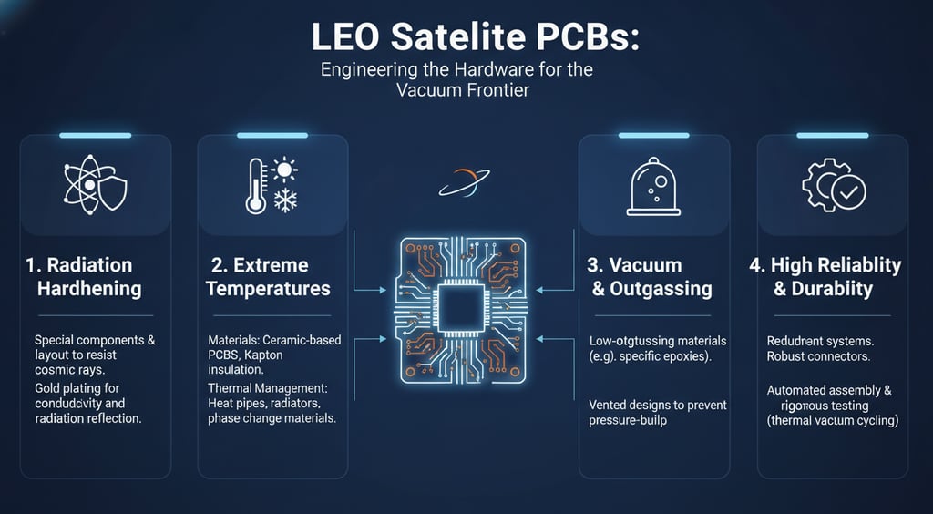
Close to Earth, LEO orbits sit between 500 and 1200 kilometers up - unlike the far-distant GEO path. Instead of distance, what really tests these spacecraft is constant change. Because one full loop takes about 90 minutes, sunlight vanishes then returns like clockwork. So heat doesn’t creep; it surges and crashes without pause. Inside, circuits face sharp swings - from deep cold below freezing to scorching highs past boiling - over and over. Sixteen cycles daily push materials to their breaking points. It's not space emptiness that wears them down - it’s the relentless rhythm of temperature shocks.
Faster shrinking and growing stresses connections deeply. Because copper lines stretch differently than resin or ceramics do, things start breaking over time. When the board swells quicker than solder spots can handle, tiny splits form - these cause spotty malfunctions you cannot fix. So picking core materials leans less on insulation traits, more on how evenly they swell up and down to save hole linings from splitting apart.
The Outgassing Imperative
Not just heat worries, but empty space brings another problem - gas escaping materials. Inside regular epoxies or coating layers, hidden chemicals start to vaporize when there’s no air pressure. Once free, those fumes won’t vanish; instead, they settle where it's chilliest across the spacecraft. Lenses and sunlight collectors? Always among the first spots where fogging shows up.
Avoiding issues means picking stuff that passes ASTM E595 - no more than 1.0% mass drop, plus CVCM under 0.1%. Some builders, like Ominipcba, who make gear for space jobs, heat up base layers hard before putting things together; this kicks out water and fumes so the material stays calm when it hits orbit.
Hybrid Stack-up Design in Material Science
Higher-frequency satellite signals now operate in bands like Ku, Ka, and V, stretching performance limits. Because of increased loss at such ranges, common circuit board materials lose effectiveness fast. Instead of blocking interference well, they soak up energy like sponges. Materials built on PTFE or LCP handle the electrical demands far better. Cost jumps sharply with those alternatives, though. Their physical structure also tends to sag under pressure during layer alignment. Precision suffers when stacking becomes unstable.
Out here, folks go for the mixed layer setup. That one pairs top and bottom radio-frequency sheets - think Rogers or Taconic - with a stiff middle made of heat-tough FR4. The outside bits handle fast signals cleanly. Inside stays strong and handles regular circuit paths without warping. Material mix keeps things stable yet speedy. Not every board does it this way, but many do when both power and structure matter. Layers stick tight through heat cycles. Signal quality holds up even under stress.
Building these mixed boards takes careful coordination. Because PTFE and epoxy react differently when heated, their curing needs don’t match. Without precise control over pressure and heat timing, hidden tensions may bend the board or split layers apart later on. Some electronics manufacturers run simulations ahead of time, tweaking each step so materials stick well while keeping shape tight enough for complex circuit patterns.
The Phased Array Challenge HDI Complexity
Flat-panel antennas set Starlink satellites apart. Instead of moving parts, these rely on electronics to aim signals. Thousands of tiny antennae cover one side of the circuit board. On the back, many small chips control how beams are shaped. Each chip links precisely to its neighbor, forming a tight network.
Every connection here stretches HDI tech beyond usual needs. Layer counts jump between fourteen and twenty, built with via systems that skip standard rules. Signals link across levels using hidden pathways - no need to pass through every layer. These shortcuts avoid leftover wire ends, troublemakers when waves get tiny.
Skin Effect and Surface Features
Frequencies creeping up toward the Ka-band push electrical current to cling just to the surface of copper wires. Because of this shift, how bumpy the metal feels matters more than before. Ordinary ED copper, built with tiny bumps on purpose so glue can stick better, ends up being far too uneven.
These days, folks designing signal paths often pick HVLP or RTF copper foils because they help radio waves move smoothly across the board. Yet, when the surface gets too polished, it sticks less firmly to surrounding layers. Making sure everything holds together means adjusting how chemicals roughen the metal - just a touch more than bare, but never so much that tiny hills slow down signals. Each change measures only millionths of a meter.
Assembly and SMT Shaping New Space
Out there among circuit traces, putting these boards together isn’t just routine SMT work anymore. Where the digital part packs in parts like a top-tier server, every piece must still hold up under flight-grade demands.
Void Free Soldering Improves Heat Transfer
Out in space, there’s no floating heat movement. Instead of rising or spreading on its own, warmth from power amps and signal chips has to travel through solid material. That path leads from the circuit board into the outer frame, which sheds heat. A key point along that route? The solder spot beneath parts like QFNs or BGAs - especially the wide metal bases. These connections handle most of the job moving heat out.
Empty spaces inside a solder connection block heat flow, leading to concentrated overheating that may destroy the silicon chip. Too much air trapped there - like what’s allowed under common IPC Class 2 rules - is risky. Instead of accepting those limits, top-tier production setups rely on vacuum-assisted reflow technology. When heat melts the solder, applying low pressure pulls out hidden gas pockets. As they shrink, the bond becomes nearly solid across the surface. Most factories building gear meant for extreme conditions follow these tighter standards without exception.
Cleanliness and Ionic Contamination
Out in space, satellite electronics pack tightly together - leaving little room between parts. Voltage levels there run especially high, which adds stress across components. When leftover flux leaves behind ions, trouble might follow. Those tiny particles can shift over time, building paths where current shouldn’t go. Dendrite growth sneaks through gaps, bridging connections that should stay apart. Eventually, unintended bridges let electricity jump where it doesn’t belong. Short circuits appear without warning, sparked by silent buildup.
Every speck matters when circuits head for orbit. Rinsing happens under intense pressure using purified water, stripping away invisible residues. Then comes lab analysis through ion scanning - no guesswork allowed. A silent threat hides in tiny forms: one grain of salt can doom years of effort. Top makers like Ominipcba build this scrutiny right into production flow, because spotless means more than shiny - it means balanced down to chemistry’s core.
Rigid Flex Combines Lightweight Design With Simplified Structure
Fuel needs shrink when the load gets lighter. A single gram less means room for extra gear that brings income. Instead of old-style wire bundles, which pack on pounds and often fail where wires meet plugs, newer methods cut mass. Weak spots vanish when connections stop relying on crushed metal joints.
Instead of bulky wiring, thin bendable parts made of polyimide link circuits inside the board layers. Inside a satellite, components tuck together like origami thanks to stiff and bendy sections joined as one. But when placing tiny parts by machine, special supports are needed so the floppy areas stay level. If those soft zones droop while applying metal paste, lines blur - leading to short connections. Designing the tools that hold them matches the difficulty of laying out the actual electronic paths.
Testing for Reliability Beyond Launch
Long before any circuit board reaches space, shaking and roaring sounds during liftoff put it under extreme stress. Testing has to look past just circuits, probing how it handles physical punishment.
Shaking things hard on purpose helps find hidden flaws fast. From the start, jolts like rocket takeoff push parts to their edge - big ones especially, like coils and fat capacitors. These hefty bits might snap loose unless glue holds them down tight. Instead of waiting, teams add epoxy under chips or around bases by hand. Only trained hands do this well - one wrong move coats pads or blocks fixes later. Even so, sticky messes can sneak in if focus slips even slightly.
The Future of Manufacturing
Out in orbit now, everyday circuit boards have swapped their handmade past for factory-line precision. What once took months to build by hand arrives in bulk, shaped by demands from low-earth satellites. These small spacecraft need parts tough enough for cars yet fine-tuned like phone networks. Merging those needs pushes production to its sharpest edge. Precision here isn’t optional - it’s baked into every layer.
Winning here does not come from blueprints alone - it comes from how precisely things are built. Stacking mixed materials smoothly, carving copper thinner than a hair, holding solder steady under vacuum heat - these make the difference. When networks swell from clusters to swarms overhead, only tight teamwork between designers and makers such as Ominipcba keeps signals strong. What matters now is not simply arrival in space, but endurance - flawless turns around Earth, again and again.
Related Articles
Contacts
Email: sales@ominipcba.com
Mobile: +86-185-7640-5228
Copyright © 2007-2026. Omini Electronics Limited. All rights reserved.
Head Office: +86-755-2357-1819
Services
Your China turnkey partner for electronics manufacturing. We bridge design to delivery by leveraging the Shenzhen electronics ecosystem for precision engineering and streamlined PCBA supply chain logistics.
Ready to Build?
Get a comprehensive quote within 24 hours.
