Phone: +86-755-2357-1819 Mobile: +86-185-7640-5228 Email: sales@ominipcba.com whatsapp: +8618576405228

Mastering Low-Loss PCB Substrates: PTFE vs. Modified Resins
Overcome signal attenuation in 5G and radar designs. Compare PTFE vs. modified epoxy laminates and master the fabrication challenges in high-frequency PCB assembly.
PCB TECHNOLOGYPCB MANUFACTURINGPCB ASSEMBLY
OminiPCBA
1/6/20266 min read
Space on the radio wave range keeps getting tighter. Moving operations higher than 6GHz into bands like 28GHz or even 77GHz changes how circuit boards behave at their core. Instead of just holding parts together, the material now shapes how signals move through them. Common FR4, used everywhere for years, turns into something that drains power rather than passing it cleanly. It behaves less like wiring and more like a barrier when things run fast.
Out here, real-world physics pushes things toward materials that lose less energy - think fluoropolymers such as PTFE or upgraded thermoset resins like altered PPO/PPE. Still, swapping one material for another doesn’t just slide into place without issues. Every step in making electronics must shift - drilling methods, how machines handle heat during soldering, right down to oven temperature patterns.
The Science Behind Signal Loss How Materials Affect It
Every now and then, signal strength fades inside a cable because metal resistance teams up with insulation flaws. Metal parts resist current more at high frequencies thanks to crowded electron movement near the surface - rough walls make it worse. Insulation soaks up power depending on how its molecules are arranged deep within. That soaking ability gets labeled Df or loss tangent, showing exactly how much wave energy turns into warmth instead of staying useful.
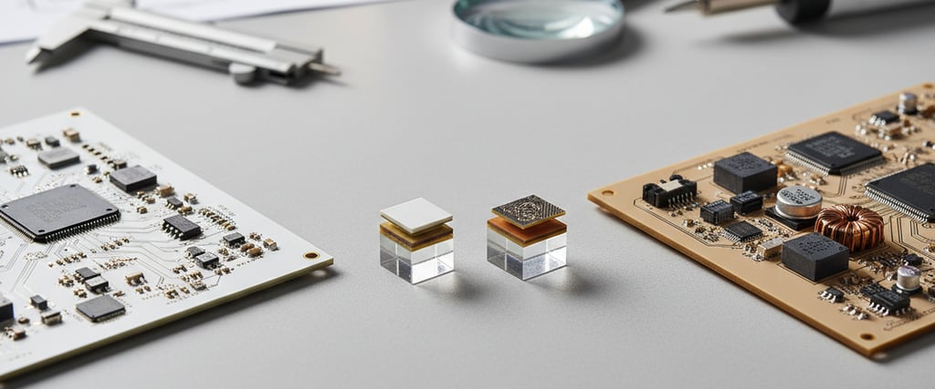
A typical FR4 material shows a dissipation factor near 0.02. At 10 Gbps speeds, such loss stays within acceptable limits. But when handling 77GHz radar waves, those losses become severe. PTFE performs much differently, reaching values down to 0.0009. That vast improvement comes because carbon-fluorine links are stiff and balanced - harder to shift under changing electrical conditions. Still, that unreactive nature - the thing giving Teflon its slick surface - brings trouble when building circuit boards. It resists sticking to copper just as much as it avoids gripping the metal lining inside drilled holes.
PTFE Troubles in Manufacturing
Dealing with old-school PTFE laminates - say, early Rogers RT/duroid types - is tricky for board makers. Heat makes this stuff go soft instead of setting hard like most materials do. When holes get drilled mechanically, rubbing creates warmth that melts the resin slightly. That goo then spreads over inner copper surfaces. Connections between layers stop working because of this film layer left behind.
Fixing this means pushing factory settings way off normal. Instead of high speed, drills turn slower while shoving more material per cut - clearing gunk before heat builds. Walls inside each hole need special treatment prior to coating. Because PTFE won’t react easily, regular cleaning fluids just sit there doing nothing. A harsh chemical, sodium naphthalene, once ruled the process - ripping fluorine from surfaces in risky fashion. These days, most shops rely on plasma instead. Hitting walls with charged gas, it roughens at microscopic levels. That texture gives copper a grip without needing reactions. Length stays fixed, just like before.
The Emergence of PTFE Similar Thermosetting Materials
Starting off, pure PTFE tends to be too soft and hard to work with. That creates issues in manufacturing where shape matters. So instead of sticking strictly to it, engineers explored alternatives. One result was tweaking thermoset resins to get closer to PTFE traits. Materials built on PPO or PPE foundations fill this role well - examples include Isola Tachyon and Panasonic Megtron. Their electrical properties come near what you’d see in PTFE setups. Yet they behave more like regular FR4 when being processed.
One thing stands out: those PTFE-style substances harden into stiff forms, holding their shape well under stress while simplifying layer alignment. Because they skip plasma treatment in numerous applications, production lines move faster with fewer steps involved. When signals run between 20 and 50GHz, such adjusted polymers tend to strike a practical middle ground - solid electrical behavior meets higher output rates. A shift is noticeable at Ominipcba, as more customers switch to composite options aiming to lower lifetime expenses yet keep data fidelity intact on fast server boards.
Copper Surface Texture and High Frequency Current Flow
Even the best insulating material won’t help when flawed metal ruins signal flow. Up in the higher frequency ranges, electrical movement sticks tight to the conductor's surface layer. When the copper side touching the layered material has an uneven texture, electrons zigzag across ridges and dips, forced to cover extra distance.
Smooth foil like VLP or HVLP copper must handle this effect. Still, such copper does not hold well when peeled. Instead of gripping through texture, the bond depends on chemistry. Because it is delicate, problems arise during full assembly. Fixing boards risks damage. Starting off, removing a part from a high-speed circuit using low-pressure copper can easily tear the connection point right off. Because of that, how carefully things are put together at first makes all the difference when trying to prevent fixes later.
The Hybrid Stack-Up Approach
One way to save money shows up when engineers build special circuit board layers. High-performance materials go just where fast signals travel. The rest of the structure relies on common FR4 stuff instead. Speed needs get premium parts. Everything else sticks with ordinary pieces. Cost stays lower without losing function.
Heat makes things grow. Yet some parts stretch faster than others. This difference causes trouble when joining certain boards together. One part pushes while another resists. The whole slab might twist during pressing. If forces get too strong, hidden connections inside break apart. Copper has to spread just right across surfaces. Material between layers needs to soak up strain like sponge. Choosing what sits in between decides if it holds or fails. Balance keeps everything flat under stress.
Glass Weave Skew A Tiny Unseen Variation
Inside the laminate, glass fabric stops acting predictable once speeds hit 25 Gbps or higher. Woven glass looks like mesh wire on a window - thick spots form where threads overlap, thin pockets appear where epoxy flows in. The glass holds a dielectric constant near 6.0, the epoxy closer to 3.0 by comparison.
One signal moves faster when traces run across different material zones - say, one above glass bundles, the other hovering over resin stretches. Timing breaks apart because of this mismatch, known as Glass Weave Skew. Flattened fiber weaves help, spreading threads thinner so gaps shrink. Another fix shifts the entire layout by around ten degrees compared to the fabric's grain. Factories handling complex boards handle that tilt automatically during manufacturing prep, evening out insulation traits across thousands of units.
Passive Intermodulation (PIM)
When it comes to radio frequency setups - like those in 5G cell towers - Passive Intermodulation matters a lot. Signals teaming up inside passive parts that don’t respond evenly can spark unwanted noise. Tiny flaws on circuit boards are often to blame: uneven edges where copper was etched, residue under protective coating, or the magnetic nature of nickel layers used in certain platings.
Vertical walls matter because uneven edges create unwanted reactions when signals get strong. One way to sidestep PIM is by using Immersion Silver or Immersion Tin instead of any coating with nickel. Shapes formed during etching need tight oversight - tiny flaws like little hooks or undercutting underneath mess things up later. Little bumps beneath the surface act strangely once power goes up.
assembly challenges at the smt frontier
Now things change once it hits the assembly line. Unlike FR4, PTFE tends to be much less rigid. Without careful control, equipment like pick-and-place units may press too hard. Board edges might show marks where conveyor rails clamp down.
When heat hits, PTFE boards can stretch fast along the vertical axis - especially without ceramic mix-ins. That sudden growth loads up vias and ball grid array connections with pressure during oven cycling. Custom heating curves help here, rolling temperature upward at a gentler pace so the slab adjusts without jerking. Stress drops when expansion spreads out instead of snapping into place.
Ceramic-loaded hydrocarbons tend to crack under stress. Because they lack the bend of raw PTFE, heavy fillers make them prone to breaking when a board bends too much - especially during separation or ICT checks. When putting together such boards, measuring strain becomes essential; it confirms whether forces stay within what the chosen layer can handle without snapping. What matters most? Staying below the break point tied to that particular material setup.
Managing Moisture During Processing
Fog gathers inside when wetness gets stuck in the material, even though PTFE pushes water away. Because certain ceramics soak it up, plus glue layers hold moisture too across stacked levels. Heat at assembly time boils that dampness into vapor, which puffs up and splits the layers apart - what some call the popcorning issue
What sets certain manufacturers apart? Baking procedures must be followed without exception. High-frequency materials cannot sit out like regular FR4 - they go straight into nitrogen-filled containers after heating. Only then do they wait, sealed, until it is time for reflow. Such tight oversight marks a builder who truly knows mmWave assembly.
Conclusion
Low-loss materials changed how circuit boards are made. Now it is less about wiring things together, more about understanding what substances do. What keeps fast electronics running - PTFE and similar versions - needs careful treatment. Handle them too hard and problems start. Chemical steps must hit exact points. Heat exposure follows its own pattern, nothing generic.
Success for a design engineer isn’t only about picking the material with top specs. It comes from knowing how well that material can actually be made into parts. A manufacturer must then back that up with proper tools and tight control over each step. When signals move faster, working closely matters more than ever. At places like Ominipcba, real talk between designers and production teams shapes what ends up working in new wireless gear. That link decides whether high-speed designs survive beyond the drawing board.
Related Articles
Contacts
Email: sales@ominipcba.com
Mobile: +86-185-7640-5228
Copyright © 2007-2026. Omini Electronics Limited. All rights reserved.
Head Office: +86-755-2357-1819
Services
Your China turnkey partner for electronics manufacturing. We bridge design to delivery by leveraging the Shenzhen electronics ecosystem for precision engineering and streamlined PCBA supply chain logistics.
Ready to Build?
Get a comprehensive quote within 24 hours.
