Phone: +86-755-2357-1819 Mobile: +86-185-7640-5228 Email: sales@ominipcba.com whatsapp: +8618576405228

IC Substrates in the Chiplet Era: The Packaging Revolution
As Chiplet technology dismantles monolithic silicon, IC substrates face critical engineering shifts. We analyze ABF materials, mSAP fabrication, and assembly risks.
PCB TECHNOLOGYPCB MANUFACTURINGPCB ASSEMBLY
OminiPCBA
1/11/20264 min read
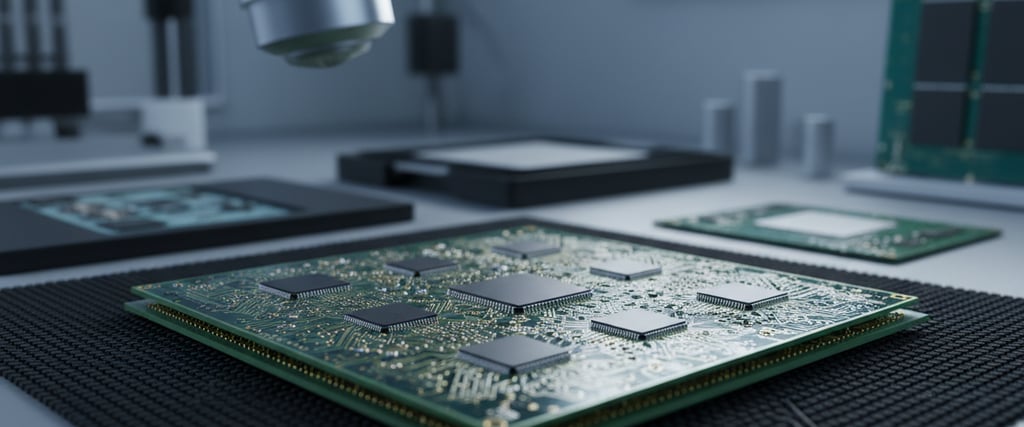
Slowing progress in transistor scaling pushed chip makers toward a new setup - swapping bulky single chips for collections of tiny chiplets. Instead of one big piece, they now link several small units, each doing its own job. This split helps improve speed while keeping expenses under control. Yet breaking things apart brings fresh challenges, especially around connections. What used to be just wiring underneath is now a complex network carrying heavy traffic. These links demand precision so tight that making them feels less like packaging and more like building circuit boards with chip-level detail.
The Shape of Difference
Now the base layer does extra work. Instead of just stretching connections out from chip to board, it links separate chips side by side. Tight clusters of inputs once only matched inside one piece of silicon now span across pieces. Speed matters more because data jumps between dies almost as fast as within them. This shift started with stacked designs that pack parts closer. Communication happens sideways through the foundation now, not just up and down. Demands grew once manufacturers glued wafers onto layered bases.
Below ten microns now - that shift pushed things forward fast. Forty by forty used to be the limit, but old HDI techniques just can’t keep up anymore. Most makers switched paths years ago - now leaning into mSAP, some even moving fully toward SAP. Instead of carving metal down like before, they grow it upward from a nearly invisible base coat. Sharp walls rise straight, helping signals stay steady when speeds climb, fitting more connections without crowding.
Material Science ABF Dominance
Firm inside parts of strong computer chips stand apart from regular circuit board stuff made with glass and epoxy. When machines handle heavy thinking tasks like artificial intelligence, they lean on a special layer called Ajinomoto Build-up Film instead. This material just works better when things heat up and move fast.
Even though it's softer to handle, ABF gives a flatter surface than glass-weave materials. Because there’s no glass inside, tiny laser-made holes can be placed more precisely. Without woven fibers, signals on fast-moving paired traces won’t slow down unevenly - something that happens when resin and glass patches scatter electrical behavior. Still, its flexible nature tends to stretch slightly when pressed together under heat. As layers stack up, small movements may occur unless tightly managed. Precision in sizing matters most at the smallest levels, especially aligning chip bump pads exactly with hidden via points below - this balance defines success in modern assembly standards tracked by groups like Omnipcba.
Heat Handling and Shape Stability
Heat builds up unevenly when chips are split into small chiplets. The main processing section can get very hot, though memory or communication parts stay cooler. Such differences in temperature push and pull on the material around them. Stress forms because one area burns while another stays calm.
When heat shifts happen, different materials react unevenly. Copper expands about 17 parts per million each degree Celsius. Silicon barely budges - just around 2.6. The organic layer stretches far more, between 20 and 50. These mismatched movements twist the base structure. Curvature mid-reflow disrupts solder connections below. Instead of clean joins, gaps appear - or unintended links form. Distortion quietly undermines reliability from within.
One way to handle this is by adding stiffener rings into the design, while spreading out copper evenly through every layer. Instead of standard methods, some teams adjust how heat moves during reflow, shaping the process around stress points. Uniform temperature matters so much that vacuum-assisted ovens or vapor-based techniques step in where regular ones fall short. These choices quietly support reliability, especially when avoiding incomplete connections becomes critical in finished circuit boards.
The Meeting of Substrate and Circuit Board SLP
Now here's something different - tiny parts inside phones and fitness trackers pushed engineers toward a new kind of circuit board called Substrate-Like PCB. Instead of just shrinking things down, it acts like a middle ground between chip carriers and regular boards. Because it borrows the fine-line methods used on silicon packaging, yet fits where bigger boards go. Though built using advanced etching tricks from microchip production, its size matches what goes into handheld gadgets.
Now tiny pathways, ultra-thin insulating layers, and packed connection points are showing up on regular circuit boards. Because of this shift, factories need much cleaner spaces to put components together. Dust levels once tolerated during normal board making can now ruin advanced assemblies with extremely narrow traces. So it’s becoming harder to tell apart traditional PCB makers from chip packaging specialists. Upgraded air purity standards and careful material handling have become unavoidable across both sides.
Interconnect Reliability Is Often the Failure Point
When wires get smaller, how they break shifts too. Tiny connections linking chip parts to the base - called micro-bumps - are usually under 20 micrometers wide. Down here, the hard mix created where metal meets surface takes up much more room inside each joint.
When temperatures shift repeatedly, these connections tend to weaken over time. Because of this, applying Underfill becomes essential - it spreads out stress that could otherwise damage the joint. This material flows into gaps between chip and board, but getting it right means carefully managing how the liquid moves. If air pockets remain trapped, heat later on might push solder around or cause tiny bursts inside the package. Companies such as Ominipcba take extra care at this stage, using sound-based imaging to check what's hidden inside. Before anything goes further, they scan for splits or missing fill just beneath the surface.
The Next Step With Glass Substrates
Down the road, organic stuff might hit its wall. Glass steps in when things get too tight. Not far off, chip builders eye flat panels made of glass. It holds shape like almost nothing else. Temperature shifts barely move it, if tuned right. Match silicon? Easily done. Super-smooth tops let tiny patterns form clean. Sharp edges stay sharp. Future stacks could rely on this clarity.
Still, glass brings fragility into play while demanding fresh approaches to metal layering. Before glass fully evolves, refining organic materials through mSAP along with next-gen insulators holds the main focus.
Conclusion
Now more than ever, chiplets have turned basic circuit boards into finely tuned systems built to match advanced chips. Signal quality and stable power rely heavily on how well these substrates are made. Getting it right means thinking about materials, exactness in etching chemicals create, and how heat moves through parts. In the world of electronic manufacturing, handling narrow margins and complex heat patterns across mixed components makes or breaks future devices.
Related Articles
Contacts
Email: sales@ominipcba.com
Mobile: +86-185-7640-5228
Copyright © 2007-2026. Omini Electronics Limited. All rights reserved.
Head Office: +86-755-2357-1819
Services
Your China turnkey partner for electronics manufacturing. We bridge design to delivery by leveraging the Shenzhen electronics ecosystem for precision engineering and streamlined PCBA supply chain logistics.
Ready to Build?
Get a comprehensive quote within 24 hours.
