Phone: +86-755-2357-1819 Mobile: +86-185-7640-5228 Email: sales@ominipcba.com whatsapp: +8618576405228

Mastering 5+ Stage HDI: The Architecture of Ultra-High-Density Interconnects
Achieving 5+N+5 HDI stackups requires mastering sequential lamination, microvia stacking, and registration accuracy. We analyze the engineering limits of ultra-high-density PCB fabrication.
PCB TECHNOLOGYPCB MANUFACTURINGPCB ASSEMBLY
OminiPCBA
1/12/20266 min read
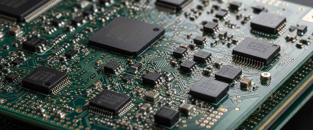
Nowhere is space tighter than inside today’s gadgets - phones, satellites, fast networks. Boards once just held parts together. Now they pack pathways into tiny three-dimensional mazes. When connections crowd closer than 0.35 millimeters, old-school holes through the board stop working. So do basic layered layouts. Instead, engineers turn to advanced stacking methods. Think five or more added levels on both sides. Or traces that jump anywhere across any layer. That shift isn’t optional - it follows where physics forces.
Building these highly intricate circuit boards goes far beyond stacking extra layers. With each new layer added, risks multiply fast - heat distortion creeps in, alignment shifts occur, chemicals behave unpredictably. Leading electronics manufacturers see a sharp break between regular production and precision nanoscale work right at the shift to five-layer construction. That fifth step isn’t just another round - it marks where ordinary techniques fall short.
The Sequential Lamination Paradox
A typical multilayer circuit board sees just one pressing. For example, a stiff 10-layer version gets all its layers joined at once under heat and pressure. But things work differently for a 5+N+5 HDI design. That kind builds up step by step. The process kicks off using a base layer - then holes get made, metal added, patterns formed. A thin insulating film goes on next - pressed into place, zapped by laser, coated with metal, then chemically shaped. Five rounds like this happen per side after that.
With each cycle, materials shift unpredictably - a tough problem engineers call material movement. When the base layer goes into the press, intense heat hits it, roughly between 180°C and 200°C, along with heavy pressure. As the epoxy hardens, it pulls inward, whereas copper pushes outward. After four prior rounds of heating, the inner sections face this again at the fifth step.
When the core changes size, guessing what it will do feels like rolling dice. A tiny shrink - just half a tenth of one percent - means laser-drilled holes land wrong, slicing past their targets so connections snap loose. Places that build complex boards, think Omnipcba's labs, fight this drift with smart math routines. After each pressing step, machines scan the board’s true shape; then update where lasers aim, syncing tools to reality instead of old blueprint numbers. What ends up matters more than what was planned.
Microvia Stacking with Copper Fill
Down near the bottom of HDI setups - say 2+N+2 - engineers tend to shift vias sideways just a bit from one layer to the next. That little move helps factories avoid trouble when coating metal across uneven holes. But once you climb into five-stage HDI territory, space gets tight fast. Trying to stagger now wastes too much room left and right. So instead, everyone lines up tiny vias straight above each other. These stacked ones build a firm column of copper through every level.
A solid stacked via starts with VIPPO - copper packed perfectly inside the pad. Instead of leaving gaps, the plating process pushes material upward through tiny laser holes. Filling happens fast from the base, avoiding trapped air by design. Success hinges on chemistry that forces complete closure without voids.
A bubble stuck in the bottom via? That spells trouble later. When heat hits fast during SMT reflow, the hidden gas pushes hard, breaking copper walls, killing electrical paths. Such flaws might hide until costly chips are already mounted. Because of that risk, precision rules every step in trusted production lines. Chemical helpers in plating baths - things like accelerants, blockers, smoothing agents - need constant watch. Their balance keeps the tiny dent at the via’s peak under 15 microns deep. A smooth seat forms then, ready for the layer above.
Laser Drilling Reaches Its Depth Limit
When layers pile up, thin spaces between them stay narrow so the whole board doesn’t get too thick or stretched out. Still, five-step HDI setups tend to blend varied insulating stuff where speed meets sturdiness.
Starting deep inside the board, a UV or CO2 laser burns through resin and glass, aiming just above the copper pad below. Hitting that mark depends less on luck and more on how short the pulse runs plus how strong it peaks. When layers stack past five, small shifts in thickness start to matter - a lot. Suppose layer 3’s prepreg swells ten microns beyond plan because resin spreads unevenly; now the beam may fall short, capped by a thin film of leftover insulation at the via base.
If the laser moves too fast, it burns past the intended spot, damaging what lies beneath. Such precision demands leave almost no room for error. Top-tier automated assembly lines show that on complex multilayer boards, beam placement stays locked within fifteen millionths of a meter across big surfaces. That level of control depends on matching alignment marks hidden inside copper layers instead of relying on outer edge drills.
Signal Behavior and Surface Currents
What makes this complicated way of building things necessary? It comes down to how signals behave. When frequencies climb into the millimeter range - needed for 5G and radar - the leftover bit of a regular plated hole begins to radiate like an antenna. That radiation bounces signals back, losing energy along the way.
Layer jumping gets smarter when stubs vanish entirely. Engineers move signals from Layer 1 straight to Layer 3 - no leftover tunnel poking through to Layer 10. Thin insulation layers pop up in five-step stacks, enabling tighter routing paths. Those narrow traces hold steady at 50 ohms, even when squeezed to 50–75 micrometers wide. Less bulk means less unwanted electrical cling and magnetic drag. Speed-hungry circuits like 112G PAM4 gear thrive because of it.
Still, there's the problem of Skin Effect. When paths on a board become thinner and copper surfaces rougher - just to stick better - the resistance goes up at higher speeds. Makers need special smooth copper layers plus chemical methods that hold things together but avoid bumpy textures messing with signals.
The Reliability Matrix Interconnect Stress Testing
A 5+ layer HDI board only works as well as its most fragile connection point. When a single device holds many hundreds - or even thousands - of layered microvias, one weak spot becomes more likely just by chance. Because copper vias expand at about 17 parts per million per degree Celsius while the nearby insulating material stretches much faster - between 40 and 60 parts per million - the difference pulls hard on the inside walls of each via. This stretch happens every time temperature shifts, never letting up.
Thermal shifts happen both while building the board and after it's running out in the real world. When heat changes hit, that thin copper coating might pull away from the pad if its grip isn’t strong enough. That kind of split inside a via shows up as what people call post separation
Checking these complicated layer builds means going past basic electrical tests. Some top makers, such as Omnipcba, turn to Interconnect Stress Testing instead. That method runs a sample board through repeated heat swings - from room temp up to 150°C - while tracking shifts in resistance on the fly. Even a small jump of 10% in resistance can mean tiny cracks are starting. From there, engineers pick materials with lower CTE values so they hold up better under stress when stacked with thick copper sections.
Yield Management and Costs
One wrong step dooms the whole batch when building complex HDI boards. Each added layer stacks more risk. Picture ten rounds of pressing and boring, every one hitting success 98 percent of the time - still, it adds up fast. Imagine tiny debris caught while fusing Layer 7. That speck? Total waste. The math tightens like a vise.
Because of this, factories make these circuit boards inside ultra-clean spaces - way cleaner than regular production floors, usually meeting Class 1000 standards or higher. Instead of waiting until the end, machines scan the surface using light, checking both the patterned copper tracks and tiny holes made by lasers, even before metal coating begins. Catching issues early through constant checks stops further work being wasted on flawed pieces.
The Future Anylayer and Substrate Like PCBs
Starting at the top, every level links through tiny vias, wiping out old lines between core and buildup. This shift brings Any-Layer HDI into view - sometimes called ELIC - where structure blurs completely. Routing jumps freely from one layer to another, skipping steps along the way. Movement happens directly, no detours needed across middle levels.
What comes before SLP boards lives in today's high-end devices. Below thirty micrometers, traces get drawn when mSAP steps in. Flagship phones hold these methods close; so do space-grade systems. Laser alignment learned here. Stacked layers stay flat because pressure got tamed across five phases. Plating fills tiny gaps without voids. Skills built on those challenges now feed what follows. This groundwork isn’t new - it just moved forward.
Conclusion
Tiny mistakes matter when building circuit boards with five or more layers. Success means pushing materials to their limits. Precision comes from combining lasers, chemistry, chemicals, and heat modeling in one tight loop. Crowded components demand flawless layer alignment. High output rates separate top makers worldwide. Making these work takes relentless attention, down to the smallest detail.
Related Articles
Contacts
Email: sales@ominipcba.com
Mobile: +86-185-7640-5228
Copyright © 2007-2026. Omini Electronics Limited. All rights reserved.
Head Office: +86-755-2357-1819
Services
Your China turnkey partner for electronics manufacturing. We bridge design to delivery by leveraging the Shenzhen electronics ecosystem for precision engineering and streamlined PCBA supply chain logistics.
Ready to Build?
Get a comprehensive quote within 24 hours.
