Phone: +86-755-2357-1819 Mobile: +86-185-7640-5228 Email: sales@ominipcba.com whatsapp: +8618576405228

Rigid-Flex PCB Dynamics: Engineering for Foldables & Bio-Wearables
Solve mechanical fatigue and impedance challenges in rigid-flex designs. Explore stackup strategies, LCP materials, and SMT assembly protocols for dynamic hinge and medical applications.
PCB TECHNOLOGYPCB MANUFACTURINGPCB ASSEMBLY
OminiPCBA
1/7/20268 min read
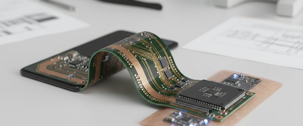
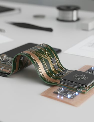
Bent but never broken - that’s how today’s gadgets roll. Twisting phones? They rely on circuits that twist too. Not long ago, these boards lived only in satellites and jets. Now they hide inside your wristband and pocket screens. Shape-shifting tech needs parts that move without failing. Signals still race through them, even when folded tight. Materials must bend yet stay strong under constant strain. Stacking layers right makes all the difference down the line. Putting it together takes more than standard tools. Science meets precision at every manufacturing step. Rigid meets flexible, then works like one piece. No room for error where motion meets electricity. These aren’t yesterday’s stiff green boards anymore. They adapt, survive, connect - quietly doing heavy lifting. Every curve carries data without missing a beat. Production lines have had to rethink old habits. Success hides in chemistry, heat, pressure, timing. What used to snap now bends thousands of times. Tiny shifts in design affect entire performance. Today’s normal was once seen as impossible.
The Spatial Paradox 3D Interconnects
Shapes used to come from circuit boards. Now gadgets bend first, forcing circuits to follow. Because devices twist, old stiff parts won’t fit anymore. Wires once snapped under stress; now flat ribbons hold strong. A single layer wraps around corners like tape. Metal traces ride inside squishy plastic sheets. Hard blocks link through soft joints that survive daily drops. Instead of bolting pieces together, everything grows from one base. Movement matters more than symmetry these days. Circuits adapt where they’re needed, not just where space allows. Failure strikes often at connections when vibration runs high. Doing away with those parts boosts how long things last before breaking. Still, that shift hands the job of staying dependable over to where the board gets made and who puts it together.
Material Physics: Polyimide vs. LCP
Picking the right insulating layer kicks off every solid rigid-flex build. Though tough when hot and easy to bend, polyimide soaks up water like a sponge - sometimes as much as three percent. Even if it handles heat well, signal strength fades faster on this stuff at high speeds because energy loss runs high. This material's been around forever, yet that doesn’t fix how dampness clings to it over time.
Foldable phones running on 50 need materials that handle huge amounts of data fast - here, Liquid Crystal Polymer stands out. Moisture hardly gets through it, soaking up less than 0.04%, plus its electrical performance stays steady even at frequencies up to 110 GHz. Yet working with it isn’t easy; bonding demands hotter presses during layering. Misalignment causes more issues compared to polyimide. Now, full-service circuit board makers are testing layered designs combining different substances: LCP carries signals quickly within bendable zones. Elsewhere, especially where parts mount firmly, older types like FR4 or Megtron stay in place.
The Neutral Bend Axis Approach
Imagine folding a phone screen thousands of days on end. That kind of motion demands precision around something called the neutral bend axis. Stretch pulls at the outside edge every time it curves. The inside edge gets squeezed instead. Right in the middle of all those layers sits an invisible line untouched by force.
Close to the middle line of bending, copper stays safer from stiffening and breaking. So place conductive paths near that central plane whenever you can. Symmetry helps achieve this balance across layers. Instead of four thin sheets stuck together tightly, two or just one layer bends far better under repeated motion. Designs built for long life tend to leave space between plies where movement happens. Unsticking them there lets each sheet shift slightly during folding. Movement spreads out stress. Bending gets easier. Cracks appear less often when parts glide instead of resisting. Stiffness drops because layers avoid locking up.
Building the Bookbinder Structure
Bending a rigid-flex circuit means the outside layers stretch more than those inside - otherwise, they might split apart. People call this the bookbinder effect, like pages fanning out at one edge. To handle it during build, flex layers get cut slightly longer step by step before getting pressed into solid parts.
Starting with the manufacturing step brings extra difficulty right away. Each inner layer gets cut slightly longer than the one before it - measurements need extreme care. A tiny error, less than a millimeter, causes wrinkles once bent, which weakens the circuit paths over time. Wrinkles become hotspots for cracks under movement. From what Omnipcba has seen, success rates depend mostly on how exact workers stack layers and whether special guides hold everything steady during pressing.
The Shift from Stiff to Flexible
Where the stiff FR4 meets the bendy PI, trouble starts. Right there, a sudden shift can slice through copper like a blade. Instead of letting that happen, people add a dab of epoxy or a clever non-drip glue along the edge. That patch spreads out the push when it bends, easing pressure across more space. One weak spot turns into a smoother handoff.
Traces crossing this edge need to run straight into it, never at a slant. When lines cut diagonally, they risk pulling apart under pressure. At every connection point between trace and pad, a teardrop form helps hold things together. Vias should stay clear of the rigid-to-flex zone by at least two millimeters. Heat shifts differently in stiff versus bendable layers, building up tension through thickness when heated. That squeeze may crack metal lining inside holes close to the boundary.
Medical wearables combining safe materials with smaller designs
Most times, speed takes a back seat when devices need to shrink down and fit skin curves. Devices like smart patches or blood sugar trackers bend with the body instead of fighting it. Tiny solid sections carry chips and sensors, spaced apart like stepping stones. These spots link through winding flexible paths that twist between them.
Curving paths shaped like loops help the circuit bend smoothly with body motion, stopping stress on delicate connections. Yet when insulating layers get extremely thin - usually under 25 micrometers - the surface mounts face trouble. Without stiffness, the material droops while applying paste. To fix that, custom vacuum trays or magnet-backed carriers keep it steady beneath the template. Uneven backing causes inconsistent deposit heights, which might create gaps or bridges under tightly spaced chips such as 0.4 millimeter ball grid arrays.
Moisture Moves Like Popcorn
Water hiding inside can wreck a rigid-flex circuit when heated too fast. Since polyimide soaks up humidity like a sponge, leaving it out in damp air adds invisible risk. A sudden jump to high heat - over 240 degrees Celsius - makes that trapped moisture flash into steam. Pressure builds before anyone notices. Layers split apart, bubbles rise under surfaces, then tiny explosions crack through the material. That violent puffing is known as popcorn damage, ending in broken connections and wasted boards.
Baking has to follow strict rules. While regular FR4 boards may only need four hours, rigid-flex types usually spend 12 to 24 hours in heat between 105°C and 125°C right before they go into production. Time runs tight once out of the oven - less than two hours passes before paste application and reflow become necessary. On better assembly lines, moisture protection steps come next; sealed bags and humidity tags move alongside boards from storage straight to placement machines without delay.
Coverlay vs. Solder Mask: The Flexibility Trade-off
Bend a flex circuit once, then see cracks form if standard LPI coating sits on top. That stiff layer does not move well when folded. Instead of that method, most designs rely on Coverlay - tough polyimide stuck down with sticky acrylic. Cracking stops because the material bends freely.
Holes form in the coverlay through drilling or laser work, letting contact points show. After that, it sticks to copper layers during lamination. Alignment tends to wander more here compared to liquid photoimageable masks. Because of this drift, openings around flexible areas need extra space - usually at least 0.1 millimeters on every edge. Tight component spacing on bendable zones often runs into trouble. Some mixed methods bring in bendable LPI as a substitute. Still, real polyimide films usually hold up better under movement and stress.
HDI Meets Microvia Integration
These days, phone circuitry needs tight spacing, so most rigid-flex designs include HDI elements like tiny holes made by lasers. Usually those small vias go where the board stays stiff. Putting them where the material bends can lead to trouble.
Thermal cycles tend to break stacked microvias in flexible areas because acrylic adhesives swell too much along the thickness direction when heated. Instead of stacking, spreading the vias out across layers works better. On solid sections of the board, placing vias inside pads saves room, which happens quite often. What matters most is how well those tiny closed-off holes get plated. Forcing fresh plating fluid into narrow cavities requires intense mixing of the chemical bath - something only the best manufacturing sites handle reliably.
Signal Integrity: Hatching vs. Solid Planes
A steady return route matters in fast rigid circuits, so makers lay down full copper sheets to block stray signals. Still, that slab of metal resists bending. Where the board must bend, engineers skip solid layers, opting instead for grid-like patterns that give the material room to move.
Even though it helps with physical durability, cross-hatching raises the transmission line's resistance while letting small amounts of electromagnetic energy escape. As a result, the return loop ends up storing more magnetic energy. To keep bending ability without losing electrical stability, engineers adjust how tightly spaced the grid lines are. Predicting delays in signal speed relies heavily on simulation software tailored to these patterns. Past builds recorded by Ominipcba show diagonal cuts at 45 degrees handle fabric layer shifts better, also making curves less sharp compared to right-angle layouts.
The Assembly Puzzle Pieces
What stands out when building rigid-flex instead of standard rigid boards? It's how much you depend on custom fixtures. Think of a rigid-flex circuit like something that acts oddly when moved - bendy, floppy, never still. Machines made for assembly need things to stay stiff and level.
Pallets made to order come out of machines that cut shapes precisely from stuff such as Durostone or aluminum, giving weak spots stability when exposed to heat waves or melting cycles. To hold the bendable parts steady, these supports might use clips pushed by springs or sticky tape built to resist extreme warmth. Heat soaks into the body of the pallet, changing how fast things warm up along the way. Because thick metal needs more power to rise in temperature, oven controls get fine-tuned - this helps molten connections form properly on circuit boards but keeps delicate flexible sections safe. Getting it right means running tests with sensors tied directly onto real boards locked inside their holders.
Inspection and Reliability Testing
When a circuit board curves even slightly, automated visual checks start to struggle. To handle small height differences across flexible sections, three-dimensional scanning tools are now more often needed. Components like QFNs and BGAs on hybrid boards require x-ray views - there is no alternative. Hidden gaps in solder joints must be caught, especially because trapped gases from adhesive layers underneath can make them worse.
Testing after building rigid-flex boards usually involves bending them repeatedly. Mounted inside a fixture, part of the batch gets flexed many times over. During this motion, electrical flow along a linked test path is watched closely. Should resistance jump suddenly, tiny cracks in the copper are likely forming. Breaking these samples proves whether the design will last through real-world use. Only by ruining units can lasting performance be truly confirmed.
The Interdisciplinary Future
A rigid-flex PCB isn’t merely a part anymore - it acts like an entire setup on its own. Getting it right means mechanical engineers, circuit designers, and production teams must actually talk to one another. How layers get pressed together matters. So does picking the right materials, not just ticking a box. Fixtures used during build aren’t afterthoughts - they decide if something lasts beyond the lab. When gadgets bend, stretch, or stick to skin, knowing how to make these boards well becomes what sets products apart. Success hides in those details most overlook at first glance.
Related Articles
Contacts
Email: sales@ominipcba.com
Mobile: +86-185-7640-5228
Copyright © 2007-2026. Omini Electronics Limited. All rights reserved.
Head Office: +86-755-2357-1819
Services
Your China turnkey partner for electronics manufacturing. We bridge design to delivery by leveraging the Shenzhen electronics ecosystem for precision engineering and streamlined PCBA supply chain logistics.
Ready to Build?
Get a comprehensive quote within 24 hours.
